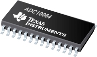

ADC10064是TI公司的一款精密ADC(<=10MSPS)产品,ADC10064是具有输入多路复用器和采样/保持功能的 10 位 600 ns A/D 转换器,本页介绍了ADC10064的产品说明、应用、特性等,并给出了与ADC10064相关的TI元器件型号供参考。
ADC10064 - 具有输入多路复用器和采样/保持功能的 10 位 600 ns A/D 转换器 - 精密ADC(<=10MSPS) - 模数转换器 - TI公司(Texas Instruments,德州仪器)
NOTE: The ADC10061 and ADC10062 are obsolete. They are described here for reference only.
Using an innovative, patented multistep* conversion technique, these CMOS analog-to-digital converters offer sub-microsecond conversion times yet dissipate a maximum of only 235mW. These converters perform 10-bit conversions in two lower-resolution “flashes”, yielding a fast A/D without the cost, power consumption, and other problems associated with true flash approaches.
The analog input voltage is sampled and held by an internal sampling circuit. Input signals at frequencies from DC to over 200kHz can, therefore, be digitized accurately without the need for an external sample-and-hold circuit.
The ADC10062 and ADC10064 include a “speed-up” pin. Connecting an external resistor between this pin and ground reduces the typical conversion time to as little as 350ns with only a small increase in linearity error.
For ease of interface to microprocessors, the ADC10061, ADC10062, and ADC10064 have been designed to appear as a memory location or I/O port without the need for external interface logic.
*U.S. Patent Number 4918449
- Built-in Sample-and-Hold
- Single +5V Supply
- No External Clock Required
- Speed Adjust Pin for Faster Conversions (ADC10062 and ADC10064). See ADC10662/4 for High Speed Ensured Performance.
Key Specifications
- Conversion Time 600 ns Typical, 900 ns Max
- Sampling Rate 800 kHz
- Low Power Dissipation 235 mW (Max)
- Total Unadjusted Error ±1.0 LSB (Max)
- No Missing Codes Over Temperature


