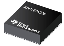

ADC10DV200是TI公司的一款高速ADC(>10MSPS)产品,ADC10DV200是具有并行 LVDS/CMOS 输出的双路 10 位、200 MSPS 低功耗 A/D 转换器,本页介绍了ADC10DV200的产品说明、应用、特性等,并给出了与ADC10DV200相关的TI元器件型号供参考。
ADC10DV200 - 具有并行 LVDS/CMOS 输出的双路 10 位、200 MSPS 低功耗 A/D 转换器 - 高速ADC(>10MSPS) - 模数转换器 - TI公司(Texas Instruments,德州仪器)
The ADC10DV200 is a monolithic analog-to-digital converter capable of converting two analog input signals into 10-bit digital words at rates up to 200 Mega Samples Per Second (MSPS). The digital output mode is selectable and can be either differential LVDS or CMOS signals. This converter uses a differential, pipelined architecture with digital error correction and an on-chip sample-and-hold circuit to minimize die size and power consumption while providing excellent dynamic performance. A unique sample-and-hold stage yields a full-power bandwidth of 900MHz. Fabricated in core CMOS process, the ADC10DV200 may be operated from a single 1.8V power supply. The ADC10DV200 achieves approximately 9.6 effective bits at Nyquist and consumes just 280mW at 170MSPS in CMOS mode and 450mW at 200MSPS in LVDS mode. The power consumption can be scaled down further by reducing sampling rates.
- Single 1.8V Power Supply Operation.
- Power Scaling with Clock Frequency.
- Internal Sample-and-Hold.
- Internal or External Reference.
- Power Down Mode.
- Offset Binary or 2's Complement Output Data Format.
- LVDS or CMOS Output Signals.
- 60-pin WQFN Package, (9x9x0.8mm, 0.5mm Pin-Pitch)
- Clock Duty Cycle Stabilizer.
- IF Sampling Bandwidth > 900MHz.
Key Specifications
- Resolution 10 Bits
- Conversion Rate 200 MSPS
- ENOB 9.6 bits (typ) @Fin=70 MHz
- SNR 59.9 dBFS (typ) @Fin=70 MHz
- SINAD 59.9 dBFS (typ) @Fin=70 MHz
- SFDR 82 dBFS (typ) @Fin=70 MHz
- LVDS Power 450mW (typ) @Fs=200 MSPS
- CMOS Power 280mW (typ) @Fs=170 MSPS
- Operating Temp. Range −40°C to +85°C.


