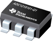

ADC121S101-Q1是TI公司的一款精密ADC(<=10MSPS)产品,ADC121S101-Q1是ADC121S101/101-Q1 单通道、0.5 至 1 Msps、12 位 A/D 转换器,本页介绍了ADC121S101-Q1的产品说明、应用、特性等,并给出了与ADC121S101-Q1相关的TI元器件型号供参考。
ADC121S101-Q1 - ADC121S101/101-Q1 单通道、0.5 至 1 Msps、12 位 A/D 转换器 - 精密ADC(<=10MSPS) - 模数转换器 - TI公司(Texas Instruments,德州仪器)
The ADC121S101 is a low-power, single channel CMOS 12-bit analog-to-digital converter with a high-speed serial interface. Unlike the conventional practice of specifying performance at a single sample rate only, the ADC121S101 is fully specified over a sample rate range of 500 ksps to 1 Msps. The converter is based upon a successive-approximation register architecture with an internal track-and-hold circuit.
The output serial data is straight binary, and is compatible with several standards, such as SPI™, QSPI™, MICROWIRE, and many common DSP serial interfaces.
The ADC121S101 operates with a single supply that can range from +2.7V to +5.25V. Normal power consumption using a +3V or +5V supply is 2.0 mW and 10 mW, respectively. The power-down feature reduces the power consumption to as low as 2.6 µW using a +5V supply.
The ADC121S101 is packaged in 6-lead WSON and SOT-23 packages. Operation over the temperature range of −40°C to +125 °C is specified.
- Specified Over a Range of Sample Rates
- 6-lead WSON and SOT-23 Packages
- Variable Power Management
- Single Power Supply with 2.7V – 5.25V Range
- SPI™/QSPI™/MICROWIRE/DSP Compatible
- AEC-Q100 Grade 1 Qualified


