
ADC128S022是TI公司的一款精密ADC(<=10MSPS)产品,ADC128S022是8 通道、50 ksps 至 200 ksps、12 位 A/D 转换器,本页介绍了ADC128S022的产品说明、应用、特性等,并给出了与ADC128S022相关的TI元器件型号供参考。
ADC128S022 - 8 通道、50 ksps 至 200 ksps、12 位 A/D 转换器 - 精密ADC(<=10MSPS) - 模数转换器 - TI公司(Texas Instruments,德州仪器)
- Eight Input Channels
- Variable Power Management
- Independent Analog and Digital Supplies
- SPI™/QSPI™/MICROWIRE/DSP Compatible
- Packaged in 16-lead TSSOP
- Conversion Rate: 50 ksps to 200ksps
- DNL (VA = VD = 5 V): +1 / −0.7 LSB (Maximum)
- INL (VA = VD = 5 V): ±1 LSB (Maximum)
- Power Consumption
- 3V Supply: 1.2 mW (Typical)
- 5V Supply: 7.5 mW (Typical)
- Automotive Navigation
- Portable Systems
- Medical Instruments
- Mobile Communications
- Instrumentation and Control Systems
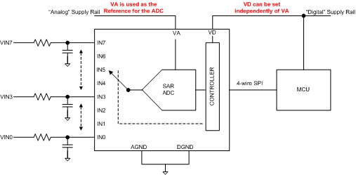
The ADC128S022 device is a low-power, eight-channel CMOS 12-bit analog-to-digital converter specified for conversion throughput rates of 50 ksps to 200 ksps. The converter is based on a successive-approximation register architecture with an internal track-and-hold circuit. It can be configured to accept up to eight input signals at inputs IN0 through IN7.
The output serial data is straight binary and is compatible with several standards, such as SPI, QSPI, MICROWIRE, and many common DSP serial interfaces.
The ADC128S022 may be operated with independent analog and digital supplies. The analog supply (VA) can range from 2.7 V to 5.25 V, and the digital supply (VD) can range from 2.7 V to VA. Normal power consumption using a 3-V or 5-V supply is 1.2 mW and 7.5 mW, respectively. The power-down feature reduces the power consumption to 0.06 µW using a 3-V supply and 0.25 µW using a 5-V supply.
The ADC128S022 is packaged in a 16-lead TSSOP package. Operation over the extended industrial temperature range of −40°C to +105°C is ensured.
| PART NUMBER | PACKAGE | BODY SIZE (NOM) |
|---|---|---|
| ADC128S022 | TSSOP (16) | 4.40 mm × 5.00 mm |


