


ADC12D1800是TI公司的一款高速模数转换器(>=1GSPS)产品,ADC12D1800是12 位、单路 3.6 GSPS 超高速 ADC,本页介绍了ADC12D1800的产品说明、应用、特性等,并给出了与ADC12D1800相关的TI元器件型号供参考。
ADC12D1800 - 12 位、单路 3.6 GSPS 超高速 ADC - 高速模数转换器(>=1GSPS) - 模数转换器 - TI公司(Texas Instruments,德州仪器)
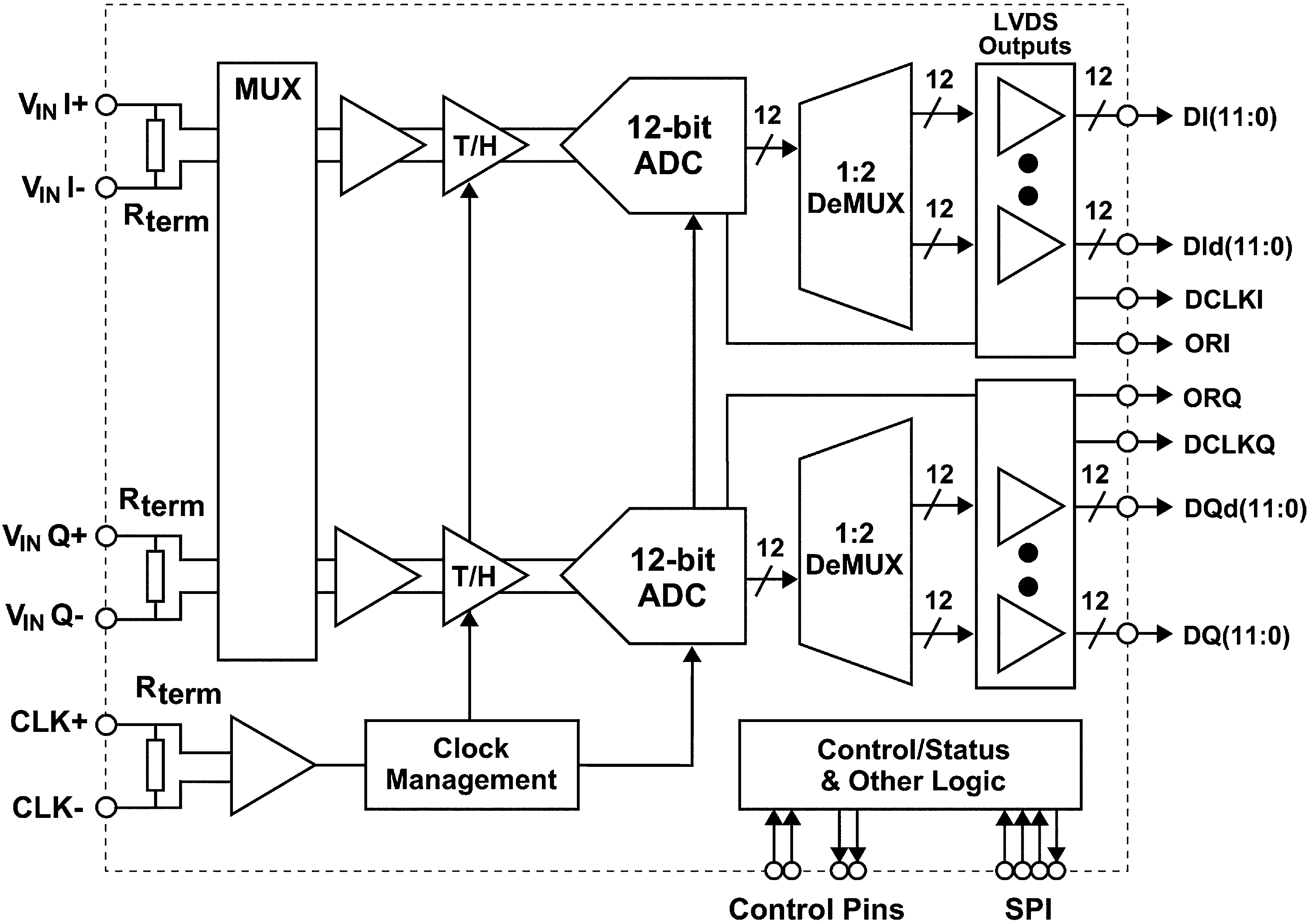
- Configurable to Either 3.6 GSPS Interleaved or 1.8 GSPS Dual ADC
- Pin-Compatible with ADC10D1000/1500 and ADC12D1000/1600
- Internally Terminated, Buffered, Differential Analog Inputs
- Interleaved Timing Automatic and Manual Skew Adjust
- Test Patterns at Output for System Debug
- Programmable 15-bit Gain and 12-bit Plus Sign Offset
- Programmable tAD Adjust Feature
- 1:1 Non-Demuxed or 1:2 Demuxed LVDS Outputs
- AutoSync Feature for Multi-Chip Systems
- Single 1.9-V ± 0.1-V Power Supply
- Key Specifications
- Resolution: 12 Bits
- Interleaved 3.6 GSPS ADC
- Noise Floor Density –153.5 dBm/Hz (typ)
- IMD3 –61 dBFS (typ)
- Noise Power Ratio 48.5 dB (typ)
- Power 4.4 W (typ)
- Full Power Bandwidth 1.75 GHz (typ)
- Dual 1.8 GSPS ADC, Fin = 125MHz
- ENOB: 9.4 (typ)
- SNR 58.5 dB (typ)
- SFDR 73 dBc (typ)
- Power 4.4 W (typ)
- Full Power Bandwidth 2.8 GHz (typ)
- Wideband Communications
- Data Acquisition Systems
- RADAR/LIDAR
- Set-top Box
- Consumer RF
- Software Defined Radio
The 12-bit, 3.6 GSPS ADC12D1800 is the latest advance in TI's Ultra-High-Speed ADC family and builds upon the features, architecture and functionality of the 10-bit GHz family of ADCs.
The ADC12D1800 provides a flexible LVDS interface which has multiple SPI programmable options to facilitate board design and FPGA/ASIC data capture. The LVDS outputs are compatible with IEEE 1596.3-1996 and supports programmable common mode voltage.
The product is packaged in a leaded or lead-free 292-ball thermally enhanced BGA package over the rated industrial temperature range of –40°C to +85°C.
To achieve full rated performance for fCLK > 1.6 GHz, write the maximum power settings one time to Register 6h through the serial interface; see Section 5.6.1 for more information.
| PART NUMBER | PACKAGE | BODY SIZE (NOM) |
|---|---|---|
| ADC12D1800 | BGA (292) | 27.00 mm × 27.00 mm |

