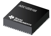

ADC12DS105是TI公司的一款高速ADC(>10MSPS)产品,ADC12DS105是具有串行 LVDS 输出的双路 12 位、105 MSPS A/D 转换器,本页介绍了ADC12DS105的产品说明、应用、特性等,并给出了与ADC12DS105相关的TI元器件型号供参考。
ADC12DS105 - 具有串行 LVDS 输出的双路 12 位、105 MSPS A/D 转换器 - 高速ADC(>10MSPS) - 模数转换器 - TI公司(Texas Instruments,德州仪器)
The ADC12DS105 is a high-performance CMOS analog-to-digital converter capable of converting two analog input signals into 12-bit digital words at rates up to 105 Mega Samples Per Second (MSPS). The digital outputs are serialized and provided on differential LVDS signal pairs. This converter uses a differential, pipelined architecture with digital error correction and an on-chip sample-and-hold circuit to minimize power consumption and the external component count, while providing excellent dynamic performance. The ADC12DS105 may be operated from a single +3.0V or 3.3V power supply. A power-down feature reduces the power consumption to very low levels while still allowing fast wake-up time to full operation. The differential inputs accept a 2V full scale differential input swing. A stable 1.2V internal voltage reference is provided, or the ADC12DS105 can be operated with an external 1.2V reference. The selectable duty cycle stabilizer maintains performance over a wide range of clock duty cycles. A serial interface allows access to the internal registers for full control of the ADC12DS105's functionality. The ADC12DS105 is available in a 60-lead WQFN package and operates over the industrial temperature range of −40°C to +85°C
- Clock Duty Cycle Stabilizer
- Single +3.0 or 3.3V Supply Operation
- Serial LVDS Outputs
- Serial Control Interface
- Overrange Outputs
- 60-pin WQFN Package, (9x9x0.8mm, 0.5mm pin-pitch)
Key Specifications
- Resolution: 12 Bits
- Conversion Rate: 105 MSPS
- SNR (fIN = 240 MHz): 68.5 dBFS (typ)
- SFDR (fIN = 240 MHz): 83 dBFS (typ)
- Full Power Bandwidth: 1 GHz (typ)
- Power Consumption: 1 W (typ)


