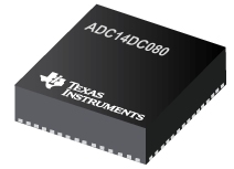

ADC14DC080是TI公司的一款高速ADC(>10MSPS)产品,ADC14DC080是具有 CMOS 输出的双路 14 位、80 MSPS A/D 转换器,本页介绍了ADC14DC080的产品说明、应用、特性等,并给出了与ADC14DC080相关的TI元器件型号供参考。
ADC14DC080 - 具有 CMOS 输出的双路 14 位、80 MSPS A/D 转换器 - 高速ADC(>10MSPS) - 模数转换器 - TI公司(Texas Instruments,德州仪器)
The ADC14DC080 is a high-performance CMOS analog-to-digital converter capable of converting two analog input signals into 14-bit digital words at rates up to 80 Mega Samples Per Second (MSPS). These converters use a differential, pipelined architecture with digital error correction and an on-chip sample-and-hold circuit to minimize power consumption and the external component count, while providing excellent dynamic performance. A unique sample-and-hold stage yields a full-power bandwidth of 1 GHz. The ADC14DC080 may be operated from a single +3.0V power supply. A power-down feature reduces the power consumption to very low levels while still allowing fast wake-up time to full operation. The differential inputs provide a 2V full scale differential input swing. A stable 1.2V internal voltage reference is provided, or the ADC14DC080 can be operated with an external 1.2V reference. Output data format (offset binary versus 2's complement) and duty cycle stabilizer are pin-selectable. The duty cycle stabilizer maintains performance over a wide range of clock duty cycles.
The ADC14DC080 is available in a 60-lead WQFN package and operates over the industrial temperature range of −40°C to +85°C.
- Internal Sample-and-Hold Circuit and Precision Reference
- Low Power Consumption
- Clock Duty Cycle Stabilizer
- Single +3.0V Supply Operation
- Power-Down Mode
- Offset Binary or 2's Complement Output Data Format
- 60-Pin WQFN Package, (9x9x0.8mm, 0.5mm Pin-Pitch)
Key Specification
- Resolution 14 Bits
- Conversion Rate 80 MSPS
- SNR (fIN = 170 MHz) 71 dBFS (typ)
- SFDR (fIN = 170 MHz) 83 dBFS (typ)
- Full Power Bandwidth 1 GHz (typ)
- Power Consumption 600 mW (typ)


