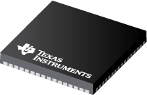

ADS42B49是TI公司的一款高速ADC(>10MSPS)产品,ADS42B49是具有模拟输入缓冲器的双通道、14 位、250MSPS 超低功率 ADC,本页介绍了ADS42B49的产品说明、应用、特性等,并给出了与ADS42B49相关的TI元器件型号供参考。
ADS42B49 - 具有模拟输入缓冲器的双通道、14 位、250MSPS 超低功率 ADC - 高速ADC(>10MSPS) - 模数转换器 - TI公司(Texas Instruments,德州仪器)
The ADS42B49 is an ultralow-power dual-channel, 14-bit analog-to-digital converter (ADC) featuring integrated analog input buffers. It uses innovative design techniques to achieve high dynamic performance, while consuming extremely low power. The presence of analog input buffers makes this device easy to drive and helps achieve high performance over a wide frequency range. The ADS42B49 is well-suited for multi-carrier, wide bandwidth communications applications.
The ADS42B49 has gain options that can be used to improve SFDR performance at lower full-scale input ranges. This device also includes a dc offset correction loop that can be used to cancel the ADC offset. Both DDR LVDS and parallel CMOS digital output interfaces are available in a compact QFN-64 PowerPAD™ package.
The device includes internal references while the traditional reference pins and associated decoupling capacitors have been eliminated. The ADS42B49 is specified over the industrial temperature range (–40°C to +85°C).
- Maximum Sample Rate: 250 MSPS
- Ultralow Power:
- 850-mW Total Power at 250 MSPS
- Integrated Analog Input Buffer:
- Input Capacitance: 2.2 pF at 170 MHz
- Input Resistance: 1.1 kΩ at 170 MHz
- High Dynamic Performance:
- 85-dBc SFDR at 170 MHz
- 70.7-dBFS SNR at 170 MHz
- Crosstalk: > 85 dB at 185 MHz
- Programmable Gain Up to 6 dB forSNR and SFDR Trade-off
- DC Offset Correction
- Output Interface Options:
- 1.8-V Parallel CMOS Interface
- Double Data Rate (DDR) LVDS with Programmable Swing:
- Standard Swing: 350 mV
- Low Swing: 200 mV
- Supports Low Input Clock AmplitudeDown to 200 mVPP
- Package: 9-mm × 9-mm, 64-Pin Quad Flat No-Lead (QFN) Package


