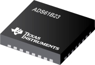

ADS61B23是TI公司的一款高速ADC(>10MSPS)产品,ADS61B23是具有缓冲差动输入的 12 位 80MSPS ADC,本页介绍了ADS61B23的产品说明、应用、特性等,并给出了与ADS61B23相关的TI元器件型号供参考。
ADS61B23 - 具有缓冲差动输入的 12 位 80MSPS ADC - 高速ADC(>10MSPS) - 模数转换器 - TI公司(Texas Instruments,德州仪器)
ADS61B23 is a 12-bit A/D converter (ADC) with a maximum sampling frequency of 80 MSPS. It combines high performance and low power consumption in a compact 32-QFN package. The analog inputs use buffers to isolate the switching transients of the internal sample & hold from the external driving circuit. The buffered inputs present very low input capacitance (< 2pF) & wide bandwidth. This makes it easy to drive them at high input frequencies, compared to an ADC without the input buffers.
ADS61B23 has coarse and fine gain options that are used to improve SFDR performance at lower full-scale analog input ranges.
The digital data outputs are parallel CMOS or DDR LVDS (Double Data Rate). Several features exist to ease data capture—controls for output clock position and output buffer drive strength, plus LVDS current and internal termination programmability.
The output interface type, gain, and other functions are programmed using a 3-wire serial interface. Alternatively, some of these functions are configured using dedicated parallel pins so the device starts in the desired state after power-up.
ADS61B23 includes internal references, while eliminating the traditional reference pins and associated external decoupling. External reference mode is also supported.
- Maximum Sample Rate: 80 MSPS
- 12-bit Resolution with No Missing Codes
- Buffered Analog Inputs with
- Very Low Input Capacitance (< 2 pF)
- High DC Resistance (5 k)
- 82 dBc SFDR and 70 dBFS SNR(-1 BFS or 1.8 Vpp input)
- 85 dBc SFDR (-6 dBFS or 1 Vpp input)
- 3.5 dB Coarse Gain and up to 6 dB Programmable Fine Gain for SNR and SFDR Trade-Off
- Parallel CMOS and Double Data Rate (DDR) LVDS Output Options
- Supports Sine, LVCMOS, LVPECL, LVDS Clock Inputs and Clock Amplitude Down to 400 mVPP
- Clock Duty Cycle Stabilizer
- Internal Reference with Support for External Reference
- External Decoupling Eliminated for References
- Programmable Output Clock Position and Drive Strength to Ease Data Capture
- 3.3 V Analog and 1.8 V to 3.3 V Digital Supply
- 32-pin QFN Package (5 mm × 5 mm)
- Pin Compatible 12-Bit Family (ADS612X)
- Temperature range -40°C to 85°C
- APPLICATIONS
- Wireless Communications Infrastructure
- Software Defined Radio
- Power Amplifier Linearization
- 802.16d/e
- Test and Measurement Instrumentation
- High Definition Video
- Medical Imaging
- Radar Systems


