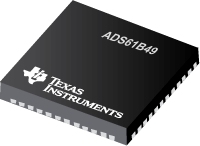

ADS61B49是TI公司的一款高速ADC(>10MSPS)产品,ADS61B49是缓冲输入、低功耗 14 位 250MSPS ADC,本页介绍了ADS61B49的产品说明、应用、特性等,并给出了与ADS61B49相关的TI元器件型号供参考。
ADS61B49 - 缓冲输入、低功耗 14 位 250MSPS ADC - 高速ADC(>10MSPS) - 模数转换器 - TI公司(Texas Instruments,德州仪器)
- Integrated High Impedance Analog Input Buffer
- Maximum Sample Rate: 250 MSPS
- 14-Bit Resolution — ADS61B49
- 12-Bit Resolution — ADS61B29
- 790 mW Total Power Dissipation at 250 MSPS
- Double Data Rate (DDR) LVDS and Parallel CMOS Output Options
- Programmable Fine Gain up to 6 dB for SNR/SFDR Trade-Off and 1-Vpp Full-Scale Operation
- DC Offset Correction
- Supports Input Clock Amplitude Down to 400 mVPP Differential
- 48-QFN Package (7mm × 7mm)
- Pin Compatible with ADS6149 Family
- APPLICATIONS
- Multicarrier, Wide Bandwidth Communications
- Wireless Multi-Carrier Communications Infrastructure
- Software Defined Radio
- Power Amplifier Linearization Feedback ADC
- 802.16d/e
- Test and Measurement Instrumentation
- High Definition Video
- Medical Imaging
- Radar Systems
DESCRIPTION
The ADS61B49 (ADS61B29) is a 14-bit (12-bit) A/D converter with a sampling rate up to 250 MSPS. It combines high dynamic performance and low power consumption in a compact 48-QFN package. An integrated analog buffer makes it well-suited for multi-carrier, wide bandwidth communications applications. The buffer maintains constant performance and input impedance across a wide frequency range.
The ADS61B49 (ADS61B29) has fine gain options that can be used to improve SFDR performance at lower full-scale input ranges. It includes a dc offset correction loop that can be used to cancel the ADC offset. Both Double Data Rate (DDR) LVDS and parallel CMOS digital output interfaces are available. At lower sampling rates, the ADC automatically operates at scaled down power with no loss in performance.
It includes internal references while the traditional reference pins and associated decoupling capacitors have been eliminated. The device is specified over the industrial temperature range (-40°C to 85°C).


