
ADS7955是TI公司的一款精密ADC(<=10MSPS)产品,ADS7955是10 位、1MSPS、8 通道、单端、微功耗、串行接口、SAR ADC,本页介绍了ADS7955的产品说明、应用、特性等,并给出了与ADS7955相关的TI元器件型号供参考。
ADS7955 - 10 位、1MSPS、8 通道、单端、微功耗、串行接口、SAR ADC - 精密ADC(<=10MSPS) - 模数转换器 - TI公司(Texas Instruments,德州仪器)
- 1-MHz Sample Rate Serial Devices
- Product Family of 12/10/8-Bit Resolution
- Zero Latency
- 20-MHz Serial Interface
- Analog Supply Range: 2.7 to 5.25 V
- I/O Supply Range: 1.7 to 5.25 V
- Two SW Selectable Unipolar, Input Ranges: 0 to 2.5 V and 0 to 5 V
- Auto and Manual Modes for Channel Selection
- 12, 8, 4-Channel Devices can Share 16 Channel Device Footprint
- Two Programmable Alarm Levels per Channel
- Four Individually Configurable GPIOs for TSSOP package devices. One GPIO for QFN devices
- Typical Power Dissipation: 14.5 mW (+VA = 5 V, +VBD = 3V) at 1 MSPS
- Power-Down Current (1 μA)
- Input Bandwidth (47 MHz at 3 dB)
- 38-,30-Pin TSSOP and 32-,24-Pin QFN Packages
- PLC / IPC
- Battery Powered Systems
- Medical Instrumentation
- Digital Power Supplies
- Touch Screen Controllers
- High-Speed Data Acquisition Systems
- High-Speed Closed-Loop Systems
The ADS79xx is a 12/10/8-bit multichannel analog-to-digital converter family. The following table shows all twelve devices from this product family.
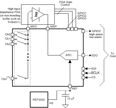
The devices include a capacitor based SAR A/D converter with inherent sample and hold.
The devices accept a wide analog supply range from 2.7 V to 5.25 V. Very low power consumption makes these devices suitable for battery-powered and isolated power supply applications.
A wide 1.7-V to 5.25-V I/O supply range facilitates a glue-less interface with the most commonly used CMOS digital hosts.
The serial interface is controlled by CS and SCLK for easy connection with microprocessors and DSP.
The input signal is sampled with the falling edge of CS. It uses SCLK for conversion, serial data output, and reading serial data in. The devices allow auto sequencing of preselected channels or manual selection of a channel for the next conversion cycle.
There are two software selectable input ranges (0 V to 2.5 V and 0 V to 5 V), four individually configurable GPIOs ( in case of TSSOP package devices), and two programmable alarm thresholds per channel. These features make the devices suitable for most data acquisition applications.
The devices offer an attractive power-down feature. This is extremely useful for power saving when the device is operated at lower conversion speeds.
The 16/12-channel devices from this family are available in a 38-pin TSSOP and 32 pin VQFN package and the 4/8-channel devices are available in a 30-pin TSSOP and 24 pin VQFN packages.
| PART NUMBER | PACKAGE | BODY SIZE (NOM) |
|---|---|---|
| ADS79xx | TSSOP (30) | 7.80 mm × 4.40 mm |
| VQFN (24) | 4.00 mm × 4.00 mm | |
| TSSOP (38) | 9.70 mm × 4.40 mm | |
| VQFN (32) | 5.00 mm × 5.00 mm |


