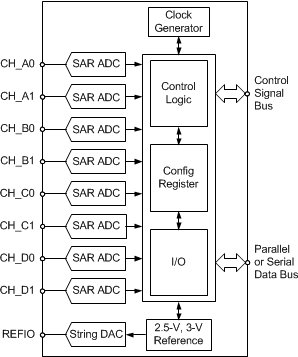

ADS8528是TI公司的一款精密ADC(<=10MSPS)产品,ADS8528是12 位、8 通道、同步采样、双极性输入 ADC,本页介绍了ADS8528的产品说明、应用、特性等,并给出了与ADS8528相关的TI元器件型号供参考。
ADS8528 - 12 位、8 通道、同步采样、双极性输入 ADC - 精密ADC(<=10MSPS) - 模数转换器 - TI公司(Texas Instruments,德州仪器)
- Family of 12-, 14-, and 16-Bit, Pin- and Software-Compatible ADCs
- Maximum Data Rate per Channel:
- ADS8528: 650 kSPS (PAR) or 480 kSPS (SER)
- ADS8548: 600 kSPS (PAR) or 450 kSPS (SER)
- ADS8568: 510 kSPS (PAR) or 400 kSPS (SER)
- Excellent AC Performance:
- Signal-to-Noise Ratio: ADS8528: 73.9 dB, ADS8548: 85 dB, ADS8568: 91.5 dB
- Total Harmonic Distortion: ADS8528: –89 dB, ADS8548: –91 dB, ADS8568: –94 dB
- Programmable, Buffered Internal Reference: 0.5 V–2.5 V or 0.5 V–3.0 V Supports Input Voltage Ranges up to ±12 V
- Selectable Parallel or Serial Interface
- Scalable Low-Power Operation Using Auto-Sleep Mode: Only 32 mW at 10 kSPS
- Fully Specified Over Extended Industrial Temperature Range
- Protection Relays
- Power Quality Measurement
- Multi-Axis Motor Controls
- Programmable Logic Controllers
- Industrial Data Acquisition
The ADS85x8 contain eight low-power, 12-, 14-, or 16-bit, successive approximation register (SAR)-based analog-to-digital converters (ADCs) with true bipolar inputs. These channels are grouped in four pairs, thus allowing simultaneous high-speed signal acquisition of up to 650 kSPS.
The devices support selectable parallel or serial interface with daisy-chain capability. The programmable reference allows handling of analog input signals with amplitudes up to ±12 V.
The ADS85x8 family supports an auto-sleep mode for minimum power dissipation and is available in both 64-pin VQFN and LQFP packages. The entire family is specified over a temperature range of –40°C to +125°C.
| PART NUMBER | PACKAGE | BODY SIZE (NOM) |
|---|---|---|
| ADS85x8 | VQFN (64) | 9.00 mm × 9.00 mm |
| LQFP (64) | 10.00 mm × 10.00 mm |


