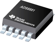

ADS8881是TI公司的一款精密ADC(<=10MSPS)产品,ADS8881是18 位、1 MSPS、串行接口、微功耗、真正差动输入 SAR ADC,本页介绍了ADS8881的产品说明、应用、特性等,并给出了与ADS8881相关的TI元器件型号供参考。
ADS8881 - 18 位、1 MSPS、串行接口、微功耗、真正差动输入 SAR ADC - 精密ADC(<=10MSPS) - 模数转换器 - TI公司(Texas Instruments,德州仪器)
- Sample Rate: 1 MHz
- No Latency Output
- Unipolar, True-Differential Input Range: –VREF to +VREF
- Wide Common-Mode Voltage Range: 0 V to VREF with 90-dB CMRR (min)
- SPI™-Compatible Serial Interface with Daisy-Chain Option
- Excellent AC and DC Performance:
- ADS8881C: INL: ±1 LSB (typ), ±2.0 LSB (max)DNL: ±1.0 LSB (max), 18-Bit NMC SNR: 100 dB, THD: –115 dB
- ADS8881I: INL: ±1.5 LSB (typ), ±3.0 LSB (max)DNL: +1.5 and –1 LSB (max), 18-Bit NMC SNR: 100 dB, THD: –115 dB
- Wide Operating Range:
- AVDD: 2.7 V to 3.6 V
- DVDD: 2.7 V to 3.6 V (Independent of AVDD)
- REF: 2.5 V to 5 V (Independent of AVDD)
- Operating Temperature: ADS8881C : 0°C to +70°C ADS8881I : –40°C to +85°C
- Low-Power Dissipation:
- 5.5 mW at 1 MSPS
- 0.55 mW at 100 kSPS
- 55 µW at 10 kSPS
- Power-Down Current (AVDD): 50 nA
- Full-Scale Step Settling to 18 Bits: 290 ns
- Packages: MSOP-10 and VSON-10
- Automatic Test Equipment (ATE)
- Instrumentation and Process Controls
- Precision Medical Equipment
- Low-Power, Battery-Operated Instruments
The ADS8881 is an 18-bit, 1-MSPS, true-differential input, analog-to-digital converter (ADC). The device operates with a 2.5-V to 5-V external reference, offering a wide selection of signal ranges without additional input signal scaling. The reference voltage setting is independent of, and can exceed, the analog supply voltage (AVDD).
The device offers an SPI-compatible serial interface that also supports daisy-chain operation for cascading multiple devices. An optional busy-indicator bit makes synchronizing with the digital host easy.
The device supports unipolar, true-differential analog input signals with a differential input swing of –VREF to VREF. This true-differential analog input structure allows for a common-mode voltage of any value in the range of 0 V to VREF (when both inputs are within the operating input range of –0.1 V to VREF + 0.1 V).
Device operation is optimized for very low-power operation. Power consumption directly scales with speed. This feature makes the ADS8881 excellent for lower-speed applications.
| PART NUMBER | PACKAGE | BODY SIZE (NOM) |
|---|---|---|
| ADS8881x | VSSOP (10) | 3.00 mm × 3.00 mm |
| VSON (10) | 3.00 mm × 3.00 mm |


