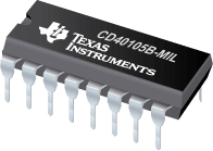

CD40105B-MIL是TI公司的一款FIFO寄存器产品,CD40105B-MIL是CMOS 4 位 x 16 字 FIFO 寄存器,本页介绍了CD40105B-MIL的产品说明、应用、特性等,并给出了与CD40105B-MIL相关的TI元器件型号供参考。
CD40105B-MIL - CMOS 4 位 x 16 字 FIFO 寄存器 - FIFO寄存器 - 触发器/锁存器/寄存器 - TI公司(Texas Instruments,德州仪器)
CD40105B is a low-power first-in-first-out (FIFO) "elastic" storage register that can store 16 4-bit words. It is capable of handling input and output data at different shifting rates. This feature makes it particularly useful as a buffer between asynchronous systems.
Each word position in the register is clocked by a control flip-flop, which stores a marker bit. A "1" signifies that the position's data is filed and a "0" denotes a vacancy in that positiion. The control flip-flop detects the state of the preceding flip-flop and communicates its own status to the succeeding flip-flop. When a control flip-flop is in the "0" state and sees a "1" in the preceding flip-flop, it generates a clock pulse that transfers data from the preceding four data latches into its own four data latches and resets the preceding flip-flop to "0". The first and last control flip-flops have buffered outputs. Since all empty locations "bubble" automatically to the input end, and all valid data ripple through to the output end, the status of the first control flip-flop (DATA-IN READY) indicates if the FIFO is full, and the status of the last flip-flop (DATA-OUT READY) indicates if the FIFO contains data. As the earliest data are removed from the bottom of the data stack (the output end), all data entered later will automatically propagate (ripple) toward the output.
Loading Data - Data can be entered whenever the DATA-IN READY (DIR) flag is high, by a low to high transition on the SHIFT-IN (SI) input. This input must go low momentarily before the next word is accepted by the FIFO. The DIR flag will go low momentarily, until the data have been transferred to the second location. The flag will remian low when all 16-word locations are filled with valid data, and further pulses on the SI input will be ignored until DIR goes high.
Unloading Data - As soon as the first work has rippled to the output, DATA-OUT READY (DOR) goes high, and data can be removed by a falling edge on the SO input. This falling edge causes the DOR signal to go low while the word on the output is dumped and the next word moves to the output. As long as valid data are available in the FIFO, the DOR signal will go high again signifying that the next word is ready at the output. When the FIFO is empty, DOR will remain low, and any further commands will be ignored until a "1" marker ripples down to the last control register, when DOR goes high. Unloading of data is inhibited while the 3-state control input is high. The 3-state control signal should not be shifted from high to low (data outputs turned on) while the SHIFT-OUT is a logic 0. This level change would cause the first word to be shifted out (unloaded) immediately and the data to be lost.
Cascading - The CD40105B can be cascaded to form longer registers simply by connecting the DIR to SO and DOR to SI. In the cascaded mode, a MASTER RESET pulse must be applied after the supply voltage is turned on. For words wider than 4 bits, the DIR and the DOR outputs must be gated together with AND gates. Their outputs drive the SI and SO inputs in paralled, if expanding is done in both directions (see Figs. 3 and 15).
3-State Outputs - In order to facilitate data busing, 3-state outputs are provided on the data output lines, while the load condition of the register can be detected by the state of the DOR output.
Master Reset - A high on the MASTER RESET (MR) sets all the contol logic marker bits to "0". DOR goes low and DIR goes high. The contents of the data register are not changed, only declared invalid, and will be superseded when the first word is loaded. The shift-in must be low during Master Reset. The CD40105B types are supplied in 16-lead hermetic dual-in-line ceramic packages (D and F suffixes), 16-lead dual-in-line plastic packages (E suffix), and in chip form (H suffix).
- Independent asynchronous inputs and outputs
- 3-state outputs
- Expandable in either direction
- Status indicators on input and output
- Reset capability
- Standardized, symmetrical output characteristics
- 100% tested for quiescent current at 20 V
- 5-V, 10-V, and 15-V parametric ratings
- Maximum input current of 1 uA at 18 V over full package-temperature range; 100 nA at 18 V and 25°C
- Noise margin (over full package-temperature range): 1V at VDD = 5V, 2V at VDD = 10 V, 2.5 V at VDD = 15 V
- Meets all requirements of JEDEC Tentative Standard No. 13B, "Standard Specifications for Description of 'B' Series CMOS Devices"
- Applications
- Bit rate smoothing
- CPU/terminal buffering
- Data communications
- Peripheral buffering
- Line printer input buffers
- Auto dialers
- CRT buffer memories
- Radar data acquisition


