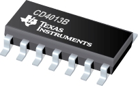

CD4013B是TI公司的一款D类触发器产品,CD4013B是CMOS 双路 D 类触发器,本页介绍了CD4013B的产品说明、应用、特性等,并给出了与CD4013B相关的TI元器件型号供参考。
CD4013B - CMOS 双路 D 类触发器 - D类触发器 - 触发器/锁存器/寄存器 - TI公司(Texas Instruments,德州仪器)
CD4013B consists of two identical, independent data-type flip-flops. Each flip-flop has independent data, set, reset, and clock inputs and Q and Q\ outputs. These devices can be used for shift register applications, and , by connecting Q\ output to the data input, for counter and toggle applications. The logic level present at the D input is transferred to the Q output during the positive-going transition of the clock pulse. Setting or resetting is independent of the clock and is accomplished by a high level on the set or rest line, respectively.
The CD4013B types are supplied in 14-lead hermetic dual-in-line ceramic packages (F3A suffix), 14-lead dual-in-line plastic packages (E suffix), 14-lead small-outline packages (M, MT, M96, and NSR suffixes), and 14-lead thin shrink small-outline packages (PW and PWR suffixes).
- Set-Reset capability
- Static flip-flop operation — retains state indefinitely with clock level either "high" or "low"
- Medium-speed operation — 16MHz (typ.) clock toggle rate at 10 V
- Standardized, symmetrical output characteristics
- 100% tested for quiescent current at 20 V
- Maximum input current of 1 µA at 18 V over full package-temperature range; 100 nA at 18 V and 25°C
- Noise margin (full package-temperature range) = 1 V at VDD = 5 V 2 V at VDD = 10 V 2.5 V at VDD = 15 V
- 5-V, 10-V, and 15-V parametric ratings
- Meets all requirements of JEDEC Tentative Standard No. 13B, "Standard Specifications for Description of ’B’ Series CMOS Devices"
- Applications:
- Registers, counters, control circuits


