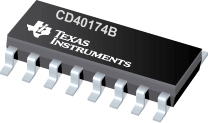

CD40174B是TI公司的一款D类触发器产品,CD40174B是CMOS 六路 D 类触发器,本页介绍了CD40174B的产品说明、应用、特性等,并给出了与CD40174B相关的TI元器件型号供参考。
CD40174B - CMOS 六路 D 类触发器 - D类触发器 - 触发器/锁存器/寄存器 - TI公司(Texas Instruments,德州仪器)
Cd40174B consists of six identical ’D’-type flip-flops having independent DATA inputs. The CLOCK and CLEAR\ inputs are common to all six units. Data are transferred to the Q outputs on the positive-going transition of the clock pulse. All sic flip-flops are simultaneously reset by a low level on the CLEAR\ input.
The CD40174B types are supplied in 16-lead hermetic dual-in-line ceramic packages (F3A suffix), 16-lead dual-in-line plastic packages (E suffix), 16-lead small-outline packages (M, M96, MT and NSR suffixes), and 16-lead thin shrink small-outline packages (PW and PWR suffixes).
- 5-V, 10-V, and 15-V parametric ratings
- Standardized, symmetrical output characteristics
- 100% tested for quiescent current at 20 V
- Maximum input current of 1 µA at 18 V over full package-temperature range; 100 nA at 18 V and 25°C
- Noise margin (full package-temperature range) = 1 V at VDD = 5 V 2 V at VDD = 10 V 2.5 V at VDD = 15 V
- Meets all requirements of JEDEC Tentative Standard No. 13B, "Standard Specifications for Description of ’B’ Series CMOS Devices"
- Applications:
- Shift Registers
- Buffer/Storage Registers
- Pattern Generators


