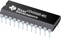

CD4508B-MIL是TI公司的一款其它锁存器产品,CD4508B-MIL是CMOS 二路 4 位锁存器,本页介绍了CD4508B-MIL的产品说明、应用、特性等,并给出了与CD4508B-MIL相关的TI元器件型号供参考。
CD4508B-MIL - CMOS 二路 4 位锁存器 - 其它锁存器 - 触发器/锁存器/寄存器 - TI公司(Texas Instruments,德州仪器)
CD4508B dual 4-bit latch contains two identical 4-bit latches with separate STROBE, RESET, and OUTPUT DISABLE control. With the STROBE line in the high state, the data on the "D" inputs appear at the corresponding "Q" outputs provided the DISABLE line is in the low state. Changing the STROBE line to the low state locks the data into the latch. A high on the reset line forces the outputs to a low level regardless of the state of the STROBE input. The outputs are forced to the high-impedance state for bus line applications by a high level on the DISABLE input.
The CD4508B types are supplied in 24-lead hermetic dual-in-line ceramic packages (F3A suffix), 24-lead dual-in-line plastic packages (E suffix), 24-lead small-outline packages (M, M96, and NSR suffixes), and 24-lead thin shrink small-outline packages (PW and PWR suffixes).
The CD4508B is similar to industry type MC14508.
- Two independent 4-bit latches
- Individual master reset for each 4-bit latch
- 3-state outputs with high-impedance state for bus line applications
- Medium-speed operation: tPHL = tPLH = 70 ns (typ.) at VDD = 10 V and CL = 50 pF
- 100% tested for quiescent current at 20 V
- 5-V, 10-V, and 15-V parametric ratings
- Standardized, symmetrical output characteristics
- Maximum input current of 1 µA at 18 V over full package-temperature range; 100 nA at 18 V and 25°C
- Noise margin (full package-temperature range) = 1 V at VDD = 5 V 2 V at VDD = 10 V 2.5 V at VDD = 15 V
- Meets all requirements of JEDEC Tentative Standard No. 13B, "Standard Specifications for Description of ’B’ Series CMOS Devices"
- Applications:
- Buffer storage
- Holding registers
- Data storage and multiplexing


