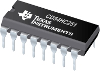

CD54HC251是TI公司的一款解码器/编码器/多路复用器产品,CD54HC251是具有三态输出的高速 CMOS 逻辑 8 输入多路复用器,本页介绍了CD54HC251的产品说明、应用、特性等,并给出了与CD54HC251相关的TI元器件型号供参考。
CD54HC251 - 具有三态输出的高速 CMOS 逻辑 8 输入多路复用器 - 解码器/编码器/多路复用器 - 特殊逻辑 - TI公司(Texas Instruments,德州仪器)
The ’HC251 and ’HCT251 are 8-channel digital multiplexers with three-state outputs, fabricated with high-speed silicon-gate CMOS technology. Together with the low power consumption of standard CMOS integrated circuits, they possess the ability to drive 10 LSTTL loads. The three-state feature makes them ideally suited for interfacing with bus lines in a bus-oriented system.
This multiplexer features both true (Y) and complement (Y\) outputs as well as an output enable (OE\) input. The OE\ must be at a low logic level to enable this device. When the OE\ input is high, both outputs are in the high-impedance state. When enabled, address information on the data select inputs determines which data input is routed to the Y and Y\ outputs. The ’HCT251 logic family is speed, function, and pin-compatible with the standard ’LS251.
- Selects One of Eight Binary Data Inputs
- Three-State Output Capability
- True and Complement Outputs
- Typical (Data to Output) Propagation Delay of 14ns at VCC = 5V, CL = 15pF, TA = 25°C
- Fanout (Over Temperature Range)
- Standard Outputs . . . . . . . . . . . . . . . 10 LSTTL Loads
- Bus Driver Outputs . . . . . . . . . . . . . 15 LSTTL Loads
- Wide Operating Temperature Range . . . -55°C to 125°C
- Balanced Propagation Delay and Transition Times
- Significant Power Reduction Compared to LSTTL Logic ICs
- Alternate Source is Philips
- HC Types
- 2V to 6V Operation
- High Noise Immunity: NIL = 30%, NIH = 30% of VCC at VCC = 5V
- HCT Types
- 4.5V to 5.5V Operation
- Direct LSTTL Input Logic Compatibility, VIL = 0.8V (Max), VIH = 2V (Min)
- CMOS Input Compatibility, Il 1µA at VOL, VOH


