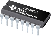

CD54HC259是TI公司的一款其它锁存器产品,CD54HC259是高速 CMOS 逻辑 8 位可寻址锁存器,本页介绍了CD54HC259的产品说明、应用、特性等,并给出了与CD54HC259相关的TI元器件型号供参考。
CD54HC259 - 高速 CMOS 逻辑 8 位可寻址锁存器 - 其它锁存器 - 触发器/锁存器/寄存器 - TI公司(Texas Instruments,德州仪器)
The ’HC259 and ’HCT259 Addressable Latch features the low-power consumption associated with CMOS circuitry and has speeds comparable to low-power Schottky.
This latches three active modes and one reset mode. When both the Latch Enable (LE\) and Master Reset (MR\) inputs are low (8-line Demultiplexer mode) the output of the addressed latch follows the Data input and all other outputs are forced low. When both MR\ and LE\ are high (Memory Mode), all outputs are isolated from the Data input, i.e., all latches hold the last data presented before the LE\ transition from low to high. A condition of LE\ low and MR\ high (Addressable Latch mode) allows the addressed latch’s output to follow the data input; all other latches are unaffected. The Reset mode (all outputs low) results when LE\ is high and MR\ is low.
- Buffered Inputs and Outputs
- Four Operating Modes
- Typical Propagation Delay of 15ns at VCC = 5V, CL = 15pF, TA = 25°C
- Fanout (Over Temperature Range) - Standard Outputs...10 LSTTL Loads - Bus Driver Outputs...15 LSTTL Loads
- Wide Operating Temperature Range... –55°C to 125°C
- Balanced Propagation Delay and Transition Times
- Significant Power Reduction Compared to LSTTL Logic ICs
- HC Types - 2V to 6V Operation - High Noise Immunity: NIL = 30%, NIH = 30% of VCC at VCC = 5V
- HCT Types - 4.5V to 5.5V Operation - Direct LSTTL Input Logic Compatibility, VIL = 0.8V (Max), VIH = 2V (Min) - CMOS Input Compatibility, Il 1µA at VOL, VOH
Data sheet acquired from Harris Semiconductor


