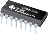

CD54HC4094是TI公司的一款移位寄存器产品,CD54HC4094是具有 3 级输出的高速 CMOS 逻辑 8 级移位和存储总线寄存器,本页介绍了CD54HC4094的产品说明、应用、特性等,并给出了与CD54HC4094相关的TI元器件型号供参考。
CD54HC4094 - 具有 3 级输出的高速 CMOS 逻辑 8 级移位和存储总线寄存器 - 移位寄存器 - 触发器/锁存器/寄存器 - TI公司(Texas Instruments,德州仪器)
The ’HC4094and CD74HCT4094 are 8-stage serial shift registers having a storage latch associated with each stage for strobing data from the serial input to parallel buffered three-stateoutputs. The parallel outputs may be connected directly to common bus lines. Data is shifted on positive clock transitions. The data in each shift register stage is transferred to the storage register when the Strobe input is high. Data in the storage register appears at the outputs whenever the Output-Enable signal is high.
Two serial outputs are available for cascading a number of these devices. Data is available at the QS1 serial output terminal on positive clock edges to allow for high-speed operation in cascaded system in which the clock rise time is fast. The same serial information, available at the QS2 terminal on the next negative clock edge, provides a means for cascading these devices when the clock rise time is slow.
- Buffered Inputs
- Separate Serial Outputs Synchronous to Both Positive and Negative Clock Edges For Cascading
- Fanout (Over Temperature Range)
- Standard Outputs. . . . . . . . . . . . . . . 10 LSTTL Loads
- Bus Driver Outputs . . . . . . . . . . . . . 15 LSTTL Loads
- Wide Operating Temperature Range . . . .–55°C to 125°C
- Balanced Propagation Delay and Transition Times
- Significant Power Reduction Compared to LSTTL Logic ICs
- HC Types
- 2V to 6V Operation
- High Noise Immunity: NIL = 30%, NIH = 30% of VCC at VCC = 5V
- HCT Types
- 4.5V to 5.5V Operation
- Direct LSTTL Input Logic Compatibility, VIL= 0.8V (Max), VIH = 2V (Min)
- CMOS Input Compatibility, Il ≤ 1µA at VOL, VOH


