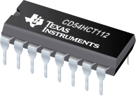

CD54HCT112是TI公司的一款J-K触发器产品,CD54HCT112是具有设置与复位功能和下降沿触发的高速 CMOS 逻辑双路 J-K 触发器,本页介绍了CD54HCT112的产品说明、应用、特性等,并给出了与CD54HCT112相关的TI元器件型号供参考。
CD54HCT112 - 具有设置与复位功能和下降沿触发的高速 CMOS 逻辑双路 J-K 触发器 - J-K触发器 - 触发器/锁存器/寄存器 - TI公司(Texas Instruments,德州仪器)
The ’HC112 and ’HCT112 utilize silicon-gate CMOS technology to achieve operating speeds equivalent to LSTTL parts. They exhibit the low power consumption of standard CMOS integrated circuits, together with the ability to drive 10 LSTTL loads.
These flip-flops have independent J, K, Set, Reset, and Clock inputs and Q and Q\ outputs. They change state on the negative-going transition of the clock pulse. Set and Reset are accomplished asynchronously by low-level inputs.
The HCT logic family is functionally as well as pin-compatible with the standard LS logic family.
- Hysteresis on Clock Inputs for Improved Noise Immunity and Increased Input Rise and Fall Times
- Asynchronous Set and Reset
- Complementary Outputs
- Buffered Inputs
- Typical fMAX = 60MHz at VCC = 5V, CL = 15pF, TA = 25°C
- Fanout (Over Temperature Range)
- Standard Outputs . . . . . 10 LSTTL Loads
- Bus Driver Outputs . . . . . 15 LSTTL Loads
- Wide Operating Temperature Range . . . –55°C to 125°C
- Balanced Propagation Delay and Transition Times
- Significant Power Reduction Compared to LSTTL Logic ICs
- HC Types
- 2V to 6V Operation
- High Noise Immunity: NIL = 30%, NIH = 30% of VCC at VCC = 5V
- HCT Types
- 4.5V to 5.5V Operation
- Direct LSTTL Input Logic Compatibility, VIL = 0.8V (Max), VIH = 2V (Min)
- CMOS Input Compatibility, Il 1µA at VOL, VOH
Data sheet acquired from Harris Semiconductor


