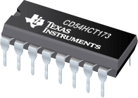

CD54HCT173是TI公司的一款D类触发器产品,CD54HCT173是具有三态输出的高速 CMOS 逻辑四路 D 类触发器,本页介绍了CD54HCT173的产品说明、应用、特性等,并给出了与CD54HCT173相关的TI元器件型号供参考。
CD54HCT173 - 具有三态输出的高速 CMOS 逻辑四路 D 类触发器 - D类触发器 - 触发器/锁存器/寄存器 - TI公司(Texas Instruments,德州仪器)
The ’HC173 and ’HCT173 high speed three-state quad Dtype flip-flops are fabricated with silicon gate CMOS technology. They possess the low power consumption of standard CMOS Integrated circuits, and can operate at speeds comparable to the equivalent low power Schottky devices. The buffered outputs can drive 15 LSTTL loads. The large output drive capability and three-state feature make these parts ideally suited for interfacing with bus lines in bus oriented systems.
The four D-type flip-flops operate synchronously from a common clock. The outputs are in the three-state mode when either of the two output disable pins are at the logic "1" level. The input ENABLES allow the flip-flops to remain in their present states without having to disrupt the clock If either of the 2 input ENABLES are taken to a logic "1" level, the Q outputs are fed back to the inputs, forcing the flip-flops to remain in the same state. Reset is enabled by taking the MASTER RESET (MR) input to a logic "1" level. The data outputs change state on the positive going edge of the clock.
The ’HCT173 logic family is functionally, as well as pin compatible with the standard LS logic family.
- Three-State Buffered Outputs
- Gated Input and Output Enables
- Fanout (Over Temperature Range)
- Standard Outputs...10 LSTTL Loads
- Bus Driver Outputs...15 LSTTL Loads
- Wide Operating Temperature Range... –55°C to 125°C
- Balanced Propagation Delay and Transition Times
- Significant Power Reduction Compared to LSTTL Logic ICs
- HC Types
- 2V to 6V Operation
- High Noise Immunity: NIL = 30%, NIH = 30% of VCC at VCC = 5V
- HCT Types
- 4.5V to 5.5V Operation
- Direct LSTTL Input Logic Compatibility, VIL = 0.8V (Max), VIH = 2V (Min)
- CMOS Input Compatibility, Il 1µA at VOL, VOH
Data sheet acquired from Harris Semiconductor


