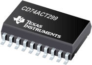

CD74ACT299是TI公司的一款移位寄存器产品,CD74ACT299是具有常见的并行 I/O 引脚和异步复位的 8 输入通用移位/存储寄存器,本页介绍了CD74ACT299的产品说明、应用、特性等,并给出了与CD74ACT299相关的TI元器件型号供参考。
CD74ACT299 - 具有常见的并行 I/O 引脚和异步复位的 8 输入通用移位/存储寄存器 - 移位寄存器 - 触发器/锁存器/寄存器 - TI公司(Texas Instruments,德州仪器)
The RCA CD54/74AC299 and CD54/74AC323 and the CD54/74ACT299 and CD54/74ACT323 are 3-state, 8-input universal shift/storage registers with common parallel I/O pins. These devices use the RCA ADVANCED CMOS technology. These registers have four synchronous-operating modes controlled by the two select inputs as shown in the Mode Select (S0, S1) table. The Mode Select, the Serial Data (DSO, DS7), and the Parallel Data (I/O0 - I/O7) respond only to the LOW-TO-HIGH transition of the clock (CP) pulse. S0, S1 and Data inputs must be present one setup time prior to the positive transition of the clock.
With the CD54/74AC/ACT 299, the Master Reset (MR\) is an asynchronous active-LOW input. When MR\ is LOW, the register is cleared regardless of the status of all other inputs. With the CD54/74AC/ACT323, the Master Reset (MR\) clears the register in sync with the clock input. The register can be expanded by cascading the same units by tying the serial output (QO) to the serial data (DS7) input of the preceding register, and tying the serial output (Q7) to the serial data (DSO) input of the following register. Recirculating the (n x 8) bits is accomplished by tying the Q7 of the last stage to the DSO of the first stage.
The 3-state input/output (I/O) port has three modes of operation:
Both Output enable (OE1\ and OE2\) inputs are LOW and S0 and S1 or both are LOW; the data in the register is present at the eight outputs. When both S0 and S1 are HIGH, I/O terminals are in the high-impedance state but being input ports, ready for parallel data to be loaded into eight registers with one clock transition regardless of the status of OE1\ and OE2\. Either one of the two Output Enable inputs being HIGH will force I/O terminals to be in the off state. It is noted that each I/O terminal is a 3-state output and a CMOS buffer input.The CD74AC/ACT299 and CD74AC/ACT323 are supplied in 20-lead dual-in-line plastic packages (E suffix) and in 20-lead dual-in-line small-outline plastic packages (M suffix). Both package types are operable over the following temperature ranges: Commercial (0 to 70°C); Industrial (-40 to +85°C); and Extended Industrial/Military (-55 to +125°C).
The CD54AC/ACT299 and CD54AC/ACT323, available in chip form (H suffix), are operable over the -55 to +125°C temperature range.
- Buffered Inputs
- Typical propagation delay: 6 ns @ VCC = 5 V, TA = 25°C, CL = 50 pF
- Exceeds 2-kV ESD Protection - MIL-STD-883, Method 3015
- SCR-Latchup-resistant CMOS process and circuit design
- Speed of bipolar FAST*/AS/S with significantly reduced power consumption
- Balanced propagation delays
- AC types feature 1.5-V to 5.5-V operation and balanced noise immunity at 30% of the supply
- ±24-mA output drive current -Fanout to 15 FAST* ICs -Drives 50-ohm transmission lines
- Characterized for operation from –40° to 85°C
*FAST is a Registered Trademark of Fairchild Semiconductor Corp.


