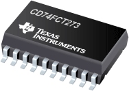

CD74FCT273是TI公司的一款D类触发器产品,CD74FCT273是具有复位功能的 BiCMOS FCT 接口逻辑八路 D 类触发器,本页介绍了CD74FCT273的产品说明、应用、特性等,并给出了与CD74FCT273相关的TI元器件型号供参考。
CD74FCT273 - 具有复位功能的 BiCMOS FCT 接口逻辑八路 D 类触发器 - D类触发器 - 触发器/锁存器/寄存器 - TI公司(Texas Instruments,德州仪器)
The CD74FCT273 is a positive-edge-triggered, D-type flip-flop with a direct clear (CLR\) input. This device uses a small-geometry BiCMOS technology. The output stage is a combination of bipolar and CMOS transistors that limits the output high level to two diode drops below VCC. This resultant lowering of output swing (0 V to 3.7 V) reduces power-bus ringing [a source of electromagnetic interference (EMI)] and minimizes VCC bounce and ground bounce and their effects during simultaneous output switching. The output configuration also enhances switching speed and is capable of sinking 48 mA.
Information at the data (D) inputs meeting the setup time requirements is transferred to the Q outputs on the positive-going edge of the clock (CLK) pulse. Clock triggering occurs at a particular voltage level and is not directly related to the transition time of the positive-going pulse. When CLK is at either the high or low level, the D input has no effect at the output. All eight flip-flops are controlled by a common clock (CLK) and a common reset (CLR\). The outputs are placed in a low state when CLR\ is taken low, independent of the CLK.
The CD74FCT273 is characterized for operation from 0°C to 70°C.
- BiCMOS Technology With Low Quiescent Power
- Buffered Inputs
- Direct Clear Input
- 48-mA Output Sink Current
- Output Voltage Swing Limited to 3.7 V
- Controlled Output Edge Rates
- Input/Output Isolation From VCC
- SCR Latch-Up-Resistant BiCMOS Process and Circuit Design
- Applications Include:
- Buffer/Storage Registers
- Shift Registers
- Pattern Generators
- Package Options Include Plastic Small-Outline (M) Package and Standard Plastic (E) DIP


