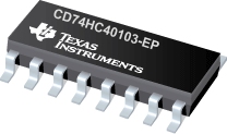

CD74HC40103-EP是TI公司的一款计数器/算术/奇偶校验功能产品,CD74HC40103-EP是增强型产品高速 Cmos 逻辑 8 级同步减计数器,本页介绍了CD74HC40103-EP的产品说明、应用、特性等,并给出了与CD74HC40103-EP相关的TI元器件型号供参考。
CD74HC40103-EP - 增强型产品高速 Cmos 逻辑 8 级同步减计数器 - 计数器/算术/奇偶校验功能 - 特殊逻辑 - TI公司(Texas Instruments,德州仪器)
The CD74HC40103 is manufactured with high-speed silicon-gate technology and consists of an 8-stage synchronous down counter with a single output, which is active when the internal count is zero. The device contains a single 8-bit binary counter. Each device has control inputs for enabling or disabling the clock, for clearing the counter to its maximum count, and for presetting the counter either synchronously or asynchronously. All control inputs and the terminal count (TC)\ output are active-low logic.
In normal operation, the counter is decremented by one count on each positive transition of the clock (CP) output. Counting is inhibited when the terminal enable (TE)\ input is high. TC\ goes low when the count reaches zero, if TE\ is low, and remains low for one full clock period.
When the synchronous preset enable (PE)\ input is low, data at the P0-P7 inputs are clocked into the counter on the next positive clock transition, regardless of the state of TE\. When the asynchronous preset enable (PL)\ input is low, data at the P0-P7 inputs asynchronously are forced into the counter, regardless of the state of the PE\, TE\, or CP inputs. Inputs P0-P7 represent a single 8-bit binary word for the CD74HC40103. When the master reset (MR)\ input is low, the counter asynchronously is cleared to its maximum count of 25510, regardless of the state of any other input. The precedence relationship between control inputs is indicated in the truth table.
If all control inputs except TE\ are high at the time of zero count, the counters jump to the maximum count, giving a counting sequence of 10016 or 25610 clock pulses long.
The CD74HC40103 may be cascaded using the TE\ input and the TC\ output in either synchronous or ripple mode. These circuits have the low power consumption usually associated with CMOS circuitry, yet have speeds comparable to low-power Schottky TTL circuits and can drive up to ten LSTTL loads.
- Controlled Baseline
- One Assembly/Test Site, One Fabrication Site
- Extended Temperature Performance of –40°C to 125°C
- Enhanced Diminishing Manufacturing Sources (DMS) Support
- Enhanced Product-Change Notification
- Qualification Pedigree
- Synchronous or Asynchronous Preset
- Cascadable in Synchronous or Ripple Mode
- Fanout (Over Temperature Range)
- Standard Outputs . . . 10 LSTTL Loads
- Bus Driver Outputs . . . 15 LSTTL Loads
- Balanced Propagation Delay and Transition Times
- Significant Power Reduction Compared to LSTTL Logic ICs
- VCC Voltage = 2 V to 6 V
- High Noise Immunity NIL or NIH = 30% of VCC, VCC = 5 V
Component qualification in accordance with JEDEC and industry standards to ensure reliable operation over an extended temperature range. This includes, but is not limited to, Highly Accelerated Stress Test (HAST) or biased 85/85, temperature cycle, autoclave or unbiased HAST, electromigration, bond intermetallic life, and mold compound life. Such qualification testing should not be viewed as justifying use of this component beyond specified performance and environmental limits.


