
CD74HC4051-EP是TI公司的一款模拟多路复用器/多路解复用器产品,CD74HC4051-EP是增强型产品高速 Cmos 逻辑模拟多路复用器/多路解复用器,本页介绍了CD74HC4051-EP的产品说明、应用、特性等,并给出了与CD74HC4051-EP相关的TI元器件型号供参考。
CD74HC4051-EP - 增强型产品高速 Cmos 逻辑模拟多路复用器/多路解复用器 - 模拟多路复用器/多路解复用器 - 多路复用器/多路解复用器(Mux/Demux) - TI公司(Texas Instruments,德州仪器)
- Controlled Baseline
- One Assembly and Test Site, One Fabrication Site
- Extended Temperature Performance of –55°C to 125°C
- Enhanced Diminishing Manufacturing Sources (DMS) Support
- Enhanced Product Change Notification
- Qualification Pedigree(1)
- Wide Analog Input Voltage Range of ±5 V Max
- Low ON-Resistance
- 70 Ω Typical (VCC – VEE = 4.5 V)
- 40 Ω Typical (VCC – VEE = 9 V)
- Low Crosstalk Between Switches
- Fast Switching and Propagation Speeds
- Break-Before-Make Switching
- Operation Control Voltage = 2 V to 6 V
- Switch Voltage = 0 V to 10 V
- High Noise Immunity NIL = 30%, NIH = 30% of VCC, VCC = 5 V (1)
Supports Defense and Aerospace Applications
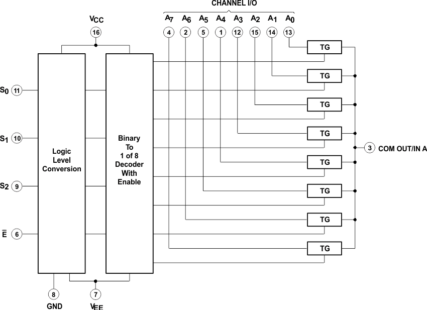
The CD74HC4051-EP is a digitally controlled analog switch that uses silicon gate CMOS technology to achieve operating speeds similar to LSTTL, with the low power consumption of standard CMOS integrated circuits.
This analog multiplexer and demultiplexer controls analog voltages that may vary across the voltage supply range (that is, VCC to VEE). These bidirectional switches allow the use of any analog input as an output and vice versa. The switches have low ON-resistance and low OFF leakages. In addition, the device has an enable control (E) that, when high, disables all switches to their OFF state.
| PART NUMBER | PACKAGE | BODY SIZE (NOM) |
|---|---|---|
| CD74HC4051-EP | SOIC (16) | 4.00 mm × 10.00 mm |


