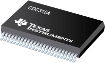

CDC318A是TI公司的一款单端产品,CDC318A是具有 I2C 控制接口的 1 线路到 18 线路时钟驱动器,本页介绍了CDC318A的产品说明、应用、特性等,并给出了与CDC318A相关的TI元器件型号供参考。
CDC318A - 具有 I2C 控制接口的 1 线路到 18 线路时钟驱动器 - 单端 - 时钟缓冲器 - TI公司(Texas Instruments,德州仪器)
The CDC318A is a high-performance clock buffer designed to distribute high-speed clocks in PC applications. This device distributes one input (A) to 18 outputs (Y) with minimum skew for clock distribution. The CDC318A operates from a 3.3-V power supply. It is characterized for operation from 0°C to 70°C.
This device has been designed with consideration for optimized EMI performance. Depending on the application layout, damping resistors in series to the clock outputs (like proposed in the PC100 specification) may not be needed in most cases.
The device provides a standard mode (100K-bits/s) I2C serial interface for device control. The implementation is as a slave/receiver. The device address is specified in the I2C device address table. Both of the I2C inputs (SDATA and SCLOCK) are 5-V tolerant and provide integrated pullup resistors (typically 140 k).
Three 8-bit I2C registers provide individual enable control for each of the outputs. All outputs default to enabled at powerup. Each output can be placed in a disabled mode with a low-level output when a low-level control bit is written to the control register. The registers are write only and must be accessed in sequential order (i.e., random access of the registers is not supported).
The CDC318A provides 3-state outputs for testing and debugging purposes. The outputs can be placed in a high-impedance state via the output-enable (OE) input. When OE is high, all outputs are in the operational state. When OE is low, the outputs are placed in a high-impedance state. OE provides an integrated pullup resistor.
- High-Speed, Low-Skew 1-to-18 Clock Buffer for Synchronous DRAM (SDRAM) Clock Buffering Applications
- Output Skew, tsk(o), Less Than 250 ps
- Pulse Skew, tsk(p), Less Than 500 ps
- Supports up to Four Unbuffered SDRAM Dual Inline Memory Modules (DIMMs)
- I2C Serial Interface Provides Individual Enable Control for Each Output
- Operates at 3.3 V
- Distributed VCC and Ground Pins Reduce Switching Noise
- 100-MHz Operation
- ESD Protection Exceeds 2000 V Per MIL-STD-883, Method 3015
- Packaged in 48-Pin Shrink Small Outline (DL) Package


