



- LM1496N - 射频和无线 > RF 其它 IC 和模块
- TLV5606CDR - 集成电路(IC) > 数据采集 > 数模转换器(DAC)
- SN74HC175NG4 - 集成电路(IC) > 逻辑 > 触发器
- PTMA402050N1AZT - 直流转换器
- 74LVC1G125DBVTE4 - 集成电路(IC) > 逻辑 > 缓冲器,驱动器,接收器,收发器
- BQ51013ARHLT - 集成电路(IC) > 电源管理(PMIC) > 电源管理 - 专用
- OPA381AIDGKT - 集成电路(IC) > 线性 > 放大器 > 仪器,运算放大器,缓冲器
- PT5101M - 板安装电源 > 直流转换器
- DS90CF364AMTD/NOPB - 集成电路(IC) > 接口 > 专用
- BQ2060ADBQ - 集成电路(IC) > 电源管理(PMIC) > 电池管理
- CY74FCT273CTSOCTE4 - 集成电路(IC) > 逻辑 > 触发器
- TPA2025D1EVM - 开发板,套件,编程器 > 评估板 > 音频放大器评估板
- LMC6574BIM - 线性器件 - 放大器 - 仪器、运算放大器、缓冲放大器
- SN74LS145NSR-P - 未分类 > 未分类
- TMS320BC53PQ80 - 集成电路(IC) > 嵌入式 > DSP(数字信号处理器)
- LM27403EVM - 开发板,套件,编程器 > 评估板 > DC/DC 和 AC/DC(离线)SMPS 评估板
- SN74ALS1035NS - 集成电路(IC) > 逻辑 > 缓冲器,驱动器,接收器,收发器
- CDCU877ARTBT - 集成电路(IC) > 时钟/定时 > 应用特定时钟/定时
- LP3917RLX-S/NOPB - 电源管理IC - 电源管理 - 专用型
- TLC3702MDR - 集成电路(IC) > 线性 > 比较器



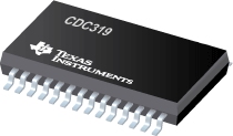
CDC319 - 具有 I2C 控制接口的 1 线路到 10 线路时钟驱动器
CDC319是TI德州仪器公司的一款单端产品,CDC319是具有 I2C 控制接口的 1 线路到 10 线路时钟驱动器,本站介绍了CDC319的封装应用图解、特点和优点、功能等,并给出了与CDC319相关的TI元器件型号供参考。
CDC319 - 具有 I2C 控制接口的 1 线路到 10 线路时钟驱动器 - 单端 - 时钟缓冲器 - 德州仪器
The CDC319 is a high-performance clock buffer that distributes one input (A) to 10 outputs (Y) with minimum skew for clock distribution. The CDC319 operates from a 3.3-V power supply, and is characterized for operation from 0°C to 70°C.
The device provides a standard mode (100K-bits/s) I2C serial interface for device control. The implementation is as a slave/receiver. The device address is specified in the I2C device address table. Both of the I2C inputs (SDATA and SCLOCK) provide integrated pullup resistors (typically 140 k) and are 5-V tolerant.
Three 8-bit I2C registers provide individual enable control for each of the outputs. All outputs default to enabled at powerup. Each output can be placed in a disabled mode with a low-level output when a low-level control bit is written to the control register. The registers are write only and must be accessed in sequential order (i.e., random access of the registers is not supported).
The CDC319 provides 3-state outputs for testing and debugging purposes. The outputs can be placed in a high-impedance state via the output-enable (OE) input. When OE is high, all outputs are in the operational state. When OE is low, the outputs are placed in a high-impedance state. OE provides an integrated pullup resistor.
- High-Speed, Low-Skew 1-to-10 Clock Buffer for SDRAM (Synchronous DRAM) Clock Buffering Applications
- Output Skew, tsk(o), Less Than 250 ps
- Pulse Skew, tsk(p), Less Than 500 ps
- Supports up to Two Unbuffered SDRAM DIMMs (Dual Inline Memory Modules)
- I2C Serial Interface Provides Individual Enable Control for Each Output
- Operates at 3.3 V
- Distributed VCC and Ground Pins Reduce Switching Noise
- ESD Protection Exceeds 2000 V Per MIL-STD-883, Method 3015
- Packaged in 28-Pin Shrink Small Outline (DB) Package
- SN6505B - SN6505x 用于隔离电源的低噪声 1A 变压器驱动器
- SN65HVD30-EP - SN65HVD30-EP, SN65HVD39-EP
- LP3855 - 1.5A 快速响应超低压降线性稳压器
- TPS3809K33-EP - TPS3809L30-EP, TPS3809K33-EP, TPS3809I50-EP
- TCA9548A - 具有复位功能的低压 8 通道 I2C 开关
- ADS1605 - 16 位 5MSPS Δ-Σ 模数转换器
- SN74LS624 - 压控振荡器
- TPS22967 - 单通道、超低电阻负载开关
- SN74LVTH574 - 具有三态输出的 3.3V ABT 八路边沿 D 类触发器
- TPS70358 - 双路输出低压降 (LDO) 稳压器

