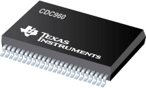

CDC960是TI公司的一款通用产品,CDC960是具有扩频和器件控制接口的 200MHz 时钟合成器/驱动器,本页介绍了CDC960的产品说明、应用、特性等,并给出了与CDC960相关的TI元器件型号供参考。
CDC960 - 具有扩频和器件控制接口的 200MHz 时钟合成器/驱动器 - 通用 - 时钟发生器 - TI公司(Texas Instruments,德州仪器)
The CDC960 is a clock synthesizer/driver and buffer that generates CPU, PCI, PCI/LDT, USB, FDC, and REF system clock signals to support PCs with an AMD-K8 Clawhammer-class system.
All output frequencies are generated from a 14.318-MHz crystal input. A reference clock input can be provided at the XIN input instead of a crystal. It is recommended to use the bypass mode of the internal oscillator in this case. Two phase-locked loops (PLLs) are used to generate the host frequencies and 48-MHz clock frequencies. On-chip loop filters and internal feedback eliminate the need for external components.
The device provides a standard mode (100 kbps) SMBus 1.1 serial interface for device control. The implementation is as a slave with read and write capability. The device address is specified in the SMBus serial interface device address table. Both SMBus inputs (SDATA and SCLK) provide integrated pullup resistors (typically 150 k).
Seven 8-bit SMBus registers provide individual enable control for each of the outputs. The controllable outputs default to enabled at power up and can be placed in a disabled mode with a low-level output when a low-level control bit is written to the control register. The registers must be accessed in sequential order (i.e., random access of the registers not supported).
The CPU, PCI, PCI_F, LDT, FDC (24/48-MHz), and USB (48-MHz) clock outputs provide low-skew/low-jitter clock signals for reliable clock operation. All outputs have 3-state capability, which can be selected via control inputs FS0, FS1, and FS2 at power-up preset condition.
The CPU bus is a 3.3-V differential push-pull output type. All others are single-ended CMOS buffers.
The host frequencies are fixed and are controlled by the FS0, FS1 and FS2 signals at power-up. The CPU bus frequencies are 200, 166, 133 and 100 MHz.
Because the CDC960 is based on PLL circuitry, it requires a stabilization time to achieve phase-lock of the PLL. With use of external reference clock, this signal must be fixed-frequency and fixed-phase prior stabilization time starts.
- Generates Clocks for AMD-K8 Clawhammer Desktop Systems
- Uses a 14.318-MHz Crystal Input to Generate Multiple Output Frequencies
- Includes Spread Spectrum Clocking (SSC), 0.5% Downspread for Reduced EMI
- Power Management Control Terminals
- SMBus Serial Interface Provides Output Enable and Control
- Low-Output Skew and Low Jitter for Clock Distribution
- Operates From Single 3.3-V Supply
- Generates the Following Clocks:
- 2 CPU (3.3 V, 180° shifted pairs, 200/166/133/100 MHz)
- 6 PCI (3.3 V, 33 MHz)
- 1 PCI_F (3.3 V, 33 MHz)
- 3 REF (3.3 V, 14.318 MHz)
- 1 USB (3.3 V, 48 MHz)
- 1 FDC (3.3 V, 24 MHz or 48 MHz)
- 3 PCI/LDT (3.3 V, 33 MHz or 66 MHz)
- Packaged in 48-Pin SSOP Package
LDT is equivalent to HT66 shown on AMD specification.


