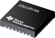

CDCLVD110A是TI公司的一款差动产品,CDCLVD110A是Progrmmable Low-Voltage 1:10 LVDS Clock Driver,本页介绍了CDCLVD110A的产品说明、应用、特性等,并给出了与CDCLVD110A相关的TI元器件型号供参考。
CDCLVD110A - Progrmmable Low-Voltage 1:10 LVDS Clock Driver - 差动 - 时钟缓冲器 - TI公司(Texas Instruments,德州仪器)
The CDCLVD110A clock driver distributes one pair of differential LVDS clock inputs (either CLK0 or CLK1) to 10 pairs of differential clock outputs (Q0–Q9) with minimum skew for clock distribution. The CDCLVD110A is specifically designed to drive 50- transmission lines.
When the control enable is high (EN = 1), the 10 differential outputs are programmable in that each output can be individually enabled/disabled (3-stated) according to the first 10 bits loaded into the shift register. Once the shift register is loaded, the last bit selects either CLK0 or CLK1 as the clock input. However, when EN = 0, the outputs are not programmable and all outputs are enabled.
The CDCLVD110A has an improved startup circuit that minimizes enabling time in AC- and DC-coupled systems.
The CDCLVD110A is characterized for operation from –40°C to 85°C.
- Low-Output Skew <30 ps (Typical) for Clock-Distribution Applications
- Distributes One Differential Clock Input to 10 LVDS Differential Clock Outputs
- VCC range 2.5 V ±5%
- Typical Signaling Rate Capability of Up to 1.1 GHz
- Configurable Register (SI/CK) Individually Enables Disables Outputs, Selectable CLK0, CLK0 or CLK1, CLK1 Inputs
- Full Rail-to-Rail Common-Mode Input Range
- Receiver Input Threshold ±100 mV
- Available in 32-Pin LQFP and QFN Package
- Fail-Safe I/O-Pins for VDD = 0 V (Power Down)
- APPLICATIONS
- General purpose Industrial, Communication and Consumer Applications


