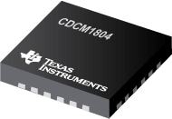

CDCM1804是TI公司的一款分频器产品,CDCM1804是1:3 LVPECL 时钟缓冲器 Addl LVCMOS 输出可编程除法器,本页介绍了CDCM1804的产品说明、应用、特性等,并给出了与CDCM1804相关的TI元器件型号供参考。
CDCM1804 - 1:3 LVPECL 时钟缓冲器 Addl LVCMOS 输出可编程除法器 - 分频器 - 时钟缓冲器 - TI公司(Texas Instruments,德州仪器)
The CDCM1804 clock driver distributes one pair of differential clock inputs to three pairs of LVPECL differential clock outputs Y[2:0] and Y[2:0], with minimum skew for clock distribution. The CDCM1804 is specifically designed for driving 50- transmission lines. Additionally, the CDCM1804 offers a single-ended LVCMOS output Y3. This output is delayed by 1.6 ns over the three LVPECL output stages to minimize noise impact during signal transitions.
The CDCM1804 has three control terminals, S0, S1, and S2, to select different output mode settings. The S[2:0] terminals are 3-level inputs and therefore allow up to 33 = 27 combinations. Additionally, an enable terminal (EN) is provided to disable or enable all outputs simultaneously. The EN terminal is a 3-level input as well and extends the number of settings to 2 × 27 = 54.
The CDCM1804 is characterized for operation from -40°C to 85°C.
For use in single-ended driver applications, the CDCM1804 also provides a VBB output terminal that can be directly connected to the unused input as a common-mode voltage reference.
- Distributes One Differential Clock Input to Three LVPECL Differential Clock Outputs and One LVCMOS Single-Ended Output
- Programmable Output Divider for Two LVPECL Outputs and LVCMOS Output
- Low-Output Skew 15 ps (Typical) for Clock-Distribution Applications for LVPECL Outputs; 1.6-ns Output Skew Between LVCMOS and LVPECL Transitions Minimizing Noise
- VCC Range 3 V-3.6 V
- Signaling Rate Up to 800-MHz LVPECL and 200-MHz LVCMOS
- Differential Input Stage for Wide Common-Mode Range
- Provides VBB Bias Voltage Output for Single-Ended Input Signals
- Receiver Input Threshold ±75 mV
- 24-Terminal QFN Package (4 mm × 4 mm)
- Accepts Any Differential Signaling: LVDS, HSTL, CML, VML, SSTL-2, and Single-Ended: LVTTL/LVCMOS


