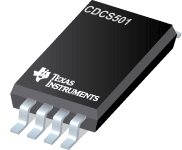

CDCS501是TI公司的一款无产品,CDCS501是具有可选展频时钟的时钟驱动器,本页介绍了CDCS501的产品说明、应用、特性等,并给出了与CDCS501相关的TI元器件型号供参考。
CDCS501 - 具有可选展频时钟的时钟驱动器 - 无 -
CDCS501 (正在供货)
The CDCS501 is a spread spectrum capable, LVCMOS Input Clock Buffer for EMI reduction.
The device is designed to counter common EMI problems in modern electronic designs.
It accepts a 3.3V LVCMOS signal at the input and spread this signal by a small amount, centered around the input frequency. The amount of spread can be selected via 3 control pins. The Functional Table contains detailed information on the amount of spread. A 4th control pin can be used to activate or deactivate the Spread Spectrum Clock Generator.
Selecting SSC_ON = off will turn the Spread Spectrum Clock Generator off only. The device will still pass the LVCMOS signal that’s presented at its input trough to its output. This pin is low active.
The wide operating frequency range covers most commonly used midrange Audio and Video frequencies. The CDCS501 operates in 3.3V environment.
It is characterized for operation from -40°C to 85°C, and available in an 8-pin TSSOP package.
- Part of a Family of Easy to use Clock Generator Devices With Optional SSC
- SSC Capable Clock Generator / Buffer
- SSC Controllable via 3 External Pins
- ±0% to ±1.5% Center Spread
- 1 External Control Pin for SSC ON / OFF Selection
- 40 MHz to 108 MHz Single-Ended LVCMOS Input
- Single 3.3V Device Power Supply
- Wide Temperature Range -40°C to 85°C
- Low Space Consumption by 8 Pin TSSOP Package
- APPLICATIONS
- Consumer and Industrial Applications Requiring EMI Reduction through Spread Spectrum Clocking


