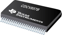

CDCV857B是TI公司的一款无产品,CDCV857B是2.5V 锁相环 DDR 时钟驱动器,本页介绍了CDCV857B的产品说明、应用、特性等,并给出了与CDCV857B相关的TI元器件型号供参考。
CDCV857B - 2.5V 锁相环 DDR 时钟驱动器 - 无 - 零延迟缓冲器 - TI公司(Texas Instruments,德州仪器)
The CDCV857B is a high-performance, low-skew, low-jitter zero delay buffer that distributes a differential clock input pair (CLK, CLK) to 10 differential pairs of clock outputs (Y[0:9], Y[0:9]) and one differential pair of feedback clock outputs (FBOUT, FBOUT). The clock outputs are controlled by the clock inputs (CLK, CLK), the feedback clocks (FBIN, FBIN), and the analog power input (AVDD). When PWRDWN is high, theoutputs switch in phase and frequency with CLK. When PWRDWN is low, all outputs are disabled to a high-impedance state (3-state) and the PLL is shut down (low-power mode). The device also enters this low-power mode when the input frequency falls below a suggested detection frequency that is below 20 MHz (typical 10 MHz). An input frequency detection circuit detects the low frequency condition and, after applying a >20-MHz input signal, this detection circuit turns the PLL on and enables the outputs.
When AVDD is strapped low, the PLL is turned off and bypassed for test purposes. The CDCV857B is also able to track spread spectrum clocking for reduced EMI.
Since the CDCV857B is based on PLL circuitry, it requires a stabilization time to achieve phase-lock of the PLL. This stabilization time is required following power up. The CDCV857B is characterized for both commercial and industrial temperature ranges.
- Phase-Lock Loop Clock Driver for Double Data-Rate Synchronous DRAM Applications
- Spread Spectrum Clock Compatible
- Operating Frequency: 60 MHz to 200 MHz
- Low Jitter (cycle-cycle): ±50 ps
- Low Static Phase Offset: ±50 ps
- Low Jitter (Period): ±35 ps
- Distributes One Differential Clock Input to 10 Differential Outputs
- Enters Low-Power Mode When No CLK Input Signal Is Applied or PWRDWN Is Low
- Operates From Dual 2.5-V Supplies
- Available in a 48-Pin TSSOP Package or 56-Ball MicroStar Junior™ BGA Package
- Consumes < 100-µA Quiescent Current
- External Feedback Pins (FBIN, FBIN) Are Used to Synchronize the Outputs to the Input Clocks
- Meets/Exceeds the Latest DDR JEDEC Spec JESD82.1


