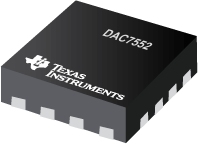

DAC7552是TI公司的一款精密DAC(=<10MSPS)产品,DAC7552是12 位、双路、超低短时脉冲波形干扰、电压输出数模转换器,本页介绍了DAC7552的产品说明、应用、特性等,并给出了与DAC7552相关的TI元器件型号供参考。
DAC7552 - 12 位、双路、超低短时脉冲波形干扰、电压输出数模转换器 - 精密DAC(=<10MSPS) - 数模转换器 - TI公司(Texas Instruments,德州仪器)
The DAC7552 is a 12-bit, dual-channel, voltage-output DAC with exceptional linearity and monotonicity. Its proprietary architecture minimizes undesired transients such as code-to-code glitch and channel-to-channel crosstalk. The low-power DAC7552 operates from a single 2.7-V to 5.5-V supply. The DAC7552 output amplifiers can drive a 2-kΩ, 200-pF load rail-to-rail with 5-µs settling time; the output range is set using an external voltage reference.
The 3-wire serial interface operates at clock rates up to 50 MHz and is compatible with SPI, QSPI, Microwire, and DSP interface standards. The outputs of all DACs may be updated simultaneously or sequentially. The parts incorporate a power-on-reset circuit to ensure that the DAC outputs power up to zero volts and remain there until a valid write cycle to the device takes place. The parts contain a power-down feature that reduces the current consumption of the device to under 2 µA.
The small size and low-power operation makes the DAC7552 ideally suited for battery-operated portable applications. The power consumption is typically 1.5 mW at 5 V, 0.75 mW at 3 V, and reduces to 1 µW in power-down mode.
The DAC7552 is available in a 16-lead QFN package and is specified over –40°C to 105°C.
- 2.7-V to 5.5-V Single Supply
- 12-Bit Linearity and Monotonicity
- Rail-to-Rail Voltage Output
- Settling Time: 5 µs (Max)
- Ultralow Glitch Energy: 0.1 nVs
- Ultralow Crosstalk: –100 dB
- Low Power: 440 µA (Max)
- Per-Channel Power Down: 2 µA (Max)
- Power-On Reset to Zero Scale
- SPI-Compatible Serial Interface: Up to 50 MHz
- Daisy-Chain Capability
- Asynchronous Hardware Clear
- Simultaneous or Sequential Update
- Specified Temperature Range: –40°C to 105°C
- Small 3-mm × 3-mm, 16-Lead QFN Package


