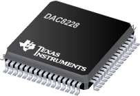

DAC8228是TI公司的一款精密DAC(=<10MSPS)产品,DAC8228是八路、低功耗、14 位 +/-16.5V 输出并行输入数模转换器,本页介绍了DAC8228的产品说明、应用、特性等,并给出了与DAC8228相关的TI元器件型号供参考。
DAC8228 - 八路、低功耗、14 位 +/-16.5V 输出并行输入数模转换器 - 精密DAC(=<10MSPS) - 数模转换器 - TI公司(Texas Instruments,德州仪器)
The DAC8228 is a low-power, octal, 14-bit digital-to-analog converter (DAC). With a 5V reference, the output can either be a bipolar ±15V voltage when operating from a dual ±15.5V (or higher) power supply, or a unipolar 0V to +30V voltage when operating from a +30.5V power supply. With a 5.5V reference, the output can be ±16.5V for a dual ±17V (or higher) power supply, or a unipolar 0V to +33V voltage when operating from a +33.5V (or higher) power supply. This DAC provides low-power operation, good linearity, and low glitch over the specified temperature range of –40°C to +105°C. This device is trimmed in manufacturing and has very low zero and full-scale error. In addition, user calibration can be performed to achieve ±1 LSB bipolar zero/full-scale error for a bipolar supply, or ±1 LSB zero-code/full-scale error for a unipolar supply over the entire signal chain. The output range can be offset by using the DAC Offset Register.
The DAC8228 features a standard, high-speed, 14-bit parallel interface that operates at up to 50MHz and is 1.8V, 3V, and 5V logic compatible, to communicate with a DSP or microprocessor. The eight DACs and the auxiliary registers are addressed with five address lines. The device features double-buffered interface logic. An asynchronous load input (LDAC) transfers data from the DAC data register to the DAC latch. The asynchronous CLR input sets the output of all eight DACs to AGND. The VMON pin is a monitor output that connects to the individual analog outputs, the offset DAC, and the reference buffer outputs through a multiplexer (mux).
The DAC8228 is pin-to-pin compatible with the DAC8728 (16-bit) and the DAC7728 (12-bit).
- Bipolar Output: ±3V, up to ±16.5V
- Unipolar Output: 0V to +33V
- 14-Bit Resolution
- Low Power: 13.5mW/Ch
- Relative Accuracy: 1LSB Max
- Flexible User Calibration
- Low Zero/Full-Scale Error
- Before User Calibration: ±2.5 LSB Max
- After User Calibration: ±1 LSB
- Low Glitch: 4nV-s
- Settling Time: 15µs
- Channel Monitor Output
- Programmable Gain: x4, x6
- Programmable Offset
- 14-Bit Parallel Interface: 50MHz (Write Operation)
- Packages: QFN-56 (8mm x 8mm), TQFP-64 (10mm x 10mm)
- APPLICATIONS
- Automatic Test Equipment
- PLC and Industrial Process Control
- Communications


