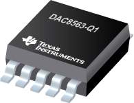

DAC8563-Q1是TI公司的一款精密DAC(=<10MSPS)产品,DAC8563-Q1是DAC8562 双路 16/14/12 位超低毛刺脉冲低功耗缓冲器电压输出 DAC,本页介绍了DAC8563-Q1的产品说明、应用、特性等,并给出了与DAC8563-Q1相关的TI元器件型号供参考。
DAC8563-Q1 - DAC8562 双路 16/14/12 位超低毛刺脉冲低功耗缓冲器电压输出 DAC - 精密DAC(=<10MSPS) - 数模转换器 - TI公司(Texas Instruments,德州仪器)
- Qualified for Automotive Applications
- AEC-Q100 Qualified with the Following Results:
- Device Temperature Grade 1: –40°C to 125°C Ambient Operating Temperature Range
- Device HBM ESD Classification Level 2
- Device CDM ESD Classification Level C4B
- Relative Accuracy:
- DAC756x (12-Bit): 0.3 LSB INL
- DAC816x (14-Bit): 1 LSB INL
- DAC856x (16-Bit): 4 LSB INL
- Glitch Impulse: 0.1 nV-s
- Bidirectional Reference: Input or 2.5-V Output
- Output Disabled by Default
- ±5-mV Initial Accuracy (Max)
- 4-ppm/°C Temperature Drift (Typ)
- 10-ppm/°C Temperature Drift (Max)
- 20-mA Sink and Source Capability
- Power-On Reset to Zero Scale or Mid-Scale
- Low-Power: 4 mW (Typ, 5-V AVDD, Including Internal Reference Current)
- Wide Power-Supply Range: 2.7 V to 5.5 V
- 50-MHz SPI With Schmitt-Triggered Inputs
- LDAC and CLR Functions
- Output Buffer With Rail-to-Rail Operation
- Package: VSSOP-10
- Portable Instrumentation
- PLC Analog Output Module
- Closed-Loop Servo Control
- Voltage Controlled Oscillator Tuning
- Data Acquisition Systems
- Programmable Gain and Offset Adjustment
The DAC756x-Q1, DAC816x-Q1, and DAC856x-Q1 (DACxx6x-Q1) devices are low-power, voltage-output, dual-channel, 12-, 14-, and 16-bit digital-to-analog converters (DACs), respectively. These devices include a 2.5-V, 4-ppm/°C internal reference, giving a full-scale output voltage range of 2.5 V or 5V. The internal reference has an initial accuracy of ±5mV and can source or sink up to 20mA at the VREFIN/VREFOUT pin.
These devices are monotonic, providing excellent linearity and minimizing undesired code-to-code transient voltages (glitch). They use a versatile three-wire serial interface that operates at clock rates up to 50 MHz. The interface is compatible with standard SPI™, QSPI™, Microwire, and digital signal processor (DSP) interfaces. The DACxx62-Q1 devices incorporate a power-on-reset circuit that ensures the DAC output powers up and remains at zero scale until a valid code is written to the device, whereas the DACxx63-Q1 devices similarly power up at mid-scale. These devices contain a power-down feature that reduces current consumption to typically 550 nA at 5V. The low power consumption, internal reference, and small footprint make these devices ideal for portable, battery-operated equipment.
The DACxx62-Q1 devices are drop-in and function-compatible with each device in this family, as are the DACxx63-Q1 devices. The entire family is available in a 10-pin VSSOP-10 (DGS) package.
| PART NUMBER | PACKAGE | BODY SIZE (NOM) |
|---|---|---|
| DAC7562-Q1 | VSSOP (10) | 3.00 mm × 3.00 mm |
| DAC7563-Q1 | ||
| DAC8162-Q1 | ||
| DAC8163-Q1 | ||
| DAC8562-Q1 | ||
| DAC8563-Q1 |


