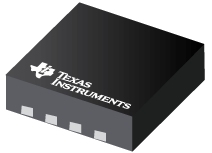

DS25BR100是TI公司的一款转接驱动器/中继器产品,DS25BR100是具有发送预强调和接收均衡功能的 3.125 Gbps LVDS 缓冲器,本页介绍了DS25BR100的产品说明、应用、特性等,并给出了与DS25BR100相关的TI元器件型号供参考。
DS25BR100 - 具有发送预强调和接收均衡功能的 3.125 Gbps LVDS 缓冲器 - 转接驱动器/中继器 - 信号调节器 - TI公司(Texas Instruments,德州仪器)
The DS25BR100 and DS25BR101 are single channel 3.125 Gbps LVDS buffers optimized for high-speed signal transmission over lossy FR-4 printed circuit board backplanes and balanced metallic cables. Fully differential signal paths ensure exceptional signal integrity and noise immunity.
The DS25BR100 and DS25BR101 feature transmit pre-emphasis (PE) and receive equalization (EQ), making them ideal for use as a repeater device. Other LVDS devices with similar IO characteristics include the following products. The DS25BR120 features four levels of pre-emphasis for use as an optimized driver device, while the DS25BR110 features four levels of equalization for use as an optimized receiver device. The DS25BR150 is a buffer/repeater with the lowest power consumption and does not feature transmit pre-emphasis nor receive equalization.
Wide input common mode range allows the receiver to accept signals with LVDS, CML and LVPECL levels; the output levels are LVDS. A very small package footprint requires minimal space on the board while the flow-through pinout allows easy board layout. On the DS25BR100 the differential input and output is internally terminated with a 100? resistor to lower return losses, reduce component count and further minimize board space. For added design flexibility the 100? input terminations on the DS25BR101 have been eliminated. This elimination enables a designer to adjust the termination for custom interconnect topologies and layout.
- DC - 3.125 Gbps Low Jitter, High Noise Immunity, Low Power Operation
- Receive Equalization Reduces ISI Jitter Due to Media Loss
- Transmit Pre-Emphasis Drives Lossy Backplanes and Cables
- On-Chip 100? Input and Output Termination:
- Minimizes Insertion and Return Losses
- Reduces Component Count
- Minimizes Board Space
- DS25BR101 Eliminates On-Chip Input Termination for Added Design Flexibility
- 7 kV ESD on LVDS I/O Pins Protects Adjoining Components
- Small 3 mm x 3 mm WSON-8 Space Saving Package


