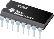

DS3658是TI公司的一款外围驱动器和传动器产品,DS3658是四路高电流外设驱动器,本页介绍了DS3658的产品说明、应用、特性等,并给出了与DS3658相关的TI元器件型号供参考。
DS3658 - 四路高电流外设驱动器 - 外围驱动器和传动器 - 其它接口 - TI公司(Texas Instruments,德州仪器)
The DS3658 quad peripheral driver is designed for those applications where low operating power, high breakdown voltage, high output current and low output ON voltage are required. A unique input circuit combines TTL compatibility with high impedance. In fact, its extreme low input current allows it to be driven directly by a CMOS device.
The outputs are capable of sinking 600 mA each and offer a 70V breakdown. However, for inductive loads the output should be clamped to 35V or less to avoid latch-up during turn off (inductive fly back protection—refer to AN-213 'SNOA610'). An on-chip clamp diode capable of handling 800 mA is provided at each output for this purpose. In addition, the DS3658 incorporates circuitry that specifies glitch-free power up or down operation and a fail-safe feature which puts the output in a high impedance state when the input is open.
The PDIP package is specifically constructed to allow increased power dissipation over conventional packages. The four ground pins are directly connected to the device chip with a special cooper lead frame. When the quad driver is soldered into a PC board, the power rating of the device improves significantly.
- Single Saturated Transistor Outputs
- Low Standby Power, 10 mW Typical
- High Impedance TTL Compatible Inputs
- Outputs May Be Tied Together for Increased Current Capacity
- High Output Current
- 600 mA Per Output
- 2.4A Per Package
- No Output Latch-up at 35V
- Low Output ON Voltage (350 mV typ @ 600 mA)
- High Breakdown Voltage (70V)
- Open Collector Outputs
- Output Clamp Diodes for Inductive Fly Back Protection
- NPN Inputs for Minimal Input Currents (1 µA Typical)
- Low Operating Power
- Standard 5V Power Supply
- Power Up/Down Protection
- Fail Safe Operation
- 2W Power Package
- Pin-for-Pin Compatible with SN75437


