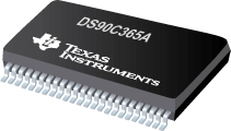

DS90C365A是TI公司的一款FlatLink/FPD-Link(用于LCD的LVDS)产品,DS90C365A是+3.3V 可编程 LVDS 发送器 18 位平板显示链接 - 87.5 MHz,本页介绍了DS90C365A的产品说明、应用、特性等,并给出了与DS90C365A相关的TI元器件型号供参考。
DS90C365A - +3.3V 可编程 LVDS 发送器 18 位平板显示链接 - 87.5 MHz - FlatLink/FPD-Link(用于LCD的LVDS) - 显示和成像串行器/解串器 - TI公司(Texas Instruments,德州仪器)
The DS90C365A is a pin to pin compatible replacement for DS90C363, DS90C363A and DS90C365. The DS90C365A has additional features and improvements making it an ideal replacement for DS90C363, DS90C363A and DS90C365. family of LVDS Transmitters.
The DS90C365A transmitter converts 21 bits of LVCMOS/LVTTL data into four LVDS (Low Voltage Differential Signaling) data streams. A phase-locked transmit clock is transmitted in parallel with the data streams over the fourth LVDS link. Every cycle of the transmit clock 21 bits RGB of input data are sampled and transmitted. At a transmit clock frequency of 87.5 MHz, 21 bits of RGB data and 3 bits of LCD timing and control data (FPLINE, FPFRAME, DRDY) are transmitted at a rate of 612.5 Mbps per LVDS data channel. Using a 87.5 MHz clock, the data throughput is 229.687 Mbytes/sec. This transmitter can be programmed for Rising edge strobe or Falling edge strobe through a dedicated pin. A Rising edge or Falling edge strobe transmitter will interoperate with a Falling edge strobe FPDLink Receiver without any translation logic.
This chipset is an ideal means to solve EMI and cable size problems associated with wide, high-speed TTL interfaces with added Spead Spectrum Clocking support..
- Pin-to-pin compatible to DS90C363, DS90C363A and DS90C365
- No special start-up sequence required between clock/data and /PD pins. Input signals (clock and data) can be applied either before or after the device is powered.
- Support Spread Spectrum Clocking up to 100kHz frequency modulation & deviations of ±2.5% center spread or -5% down spread.
- “Input Clock Detection” feature will pull all LVDS pairs to logic low when input clock is missing and when /PD pin is logic high.
- 18 to 87.5 MHz shift clock support
- Tx power consumption < 146 mW (typ) at 87.5 MHz Grayscale
- Tx Power-down mode < 37 uW (typ)
- Supports VGA, SVGA, XGA, SXGA (dual pixel), SXGA+ (dual pixel), UXGA (dual pixel).
- Narrow bus reduces cable size and cost
- Up to 1.785 Gbps throughput
- Up to 223.125 Megabytes/sec bandwidth
- 345 mV (typ) swing LVDS devices for low EMI
- PLL requires no external components
- Compliant to TIA/EIA-644 LVDS standard
- Low profile 48-lead TSSOP package
All trademarks are the property of their respective owners. TRI-STATE is a trademark of Texas Instruments. TRI-STATE is a trademark of Texas Instruments.


