


LM53601-Q1是TI公司的一款转换器(集成开关)产品,LM53601-Q1是面向汽车类应用的 3.5V 至 36V、1A 同步 2.1MHz 降压转换器,本页介绍了LM53601-Q1的产品说明、应用、特性等,并给出了与LM53601-Q1相关的TI元器件型号供参考。
LM53601-Q1 - 面向汽车类应用的 3.5V 至 36V、1A 同步 2.1MHz 降压转换器 - 转换器(集成开关) - DC/DC开关稳压器 - TI公司(Texas Instruments,德州仪器)
- Automotive Grade Product, AEC Grade 1 Qualified
- 10-lead 3 mm x 3 mm WSON Package
- –40°C to 150°C junction Temperature Range
- Peak Current Mode Control
- 2.1-MHz (±10%) Fixed Switching Frequency
- Pin Selectable Forced PWM Mode
- External Frequency Synchronization With Forced PWM Mode
- Reset Output With Filter and Delayed Release
- Automatic Light Load Mode for Improved Efficiency
- Built-In Compensation, Soft-start, Current Limit, Thermal Shutdown, and UVLO
- Spread Spectrum is Available as a Factory Option
- Electrical Specifications
- 3.5-V to 36 V Input Voltage With Transients up to 42 V
- 1000-mA Maximum Load Current (LM53601-Q1)
- 650-mA Maximum load Current (LM53600-Q1)
- Output Voltage Options: 5 V, 3.3 V, and Adjustable
- ±2% Fixed Output Voltage Tolerance (Over Temperature)
- ±1.75% FB Voltage Tolerance for Adjustable Output Version (Over Temperature)
- 1.8-µA Current When Shutdown (Typical)
- 22-µA Quiescent Current at No Load With 3.3-V Output (Typical)
space
- Automotive Camera Applications
- Automotive Infotainment
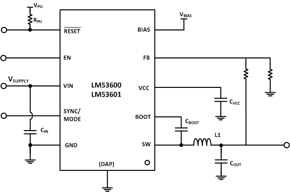
The LM53600/01 synchronous buck regulator is optimized for automotive applications, providing either an adjustable output or an output voltage of 3.3 V or 5 V. The LM53600-Q1 device supports load currents up to 650 mA and the LM536001-Q1 supports load currents up to 1000 mA.
Advanced high speed circuitry allows the device to regulate from an 18-V input to a 3.3-V output at a fixed frequency of 2.1 MHz. Innovative architecture allows the device to regulate a 3.3-V output from an input voltage of only 3.8 V. Input voltage range up to 36 V, with transient tolerance up to 42 V, eases input surge protection design.
An open drain reset output, with filtering and delayed release, provides a true indication of system status. This feature negates the requirement for an additional supervisory component, saving cost and board space. Seamless transition between PWM and PFM modes, along with a quiescent current of only 22 µA, ensures high efficiency and superior transient response at all loads. Few external components are needed allowing the generation of compact PCB layout. The device characteristics are specified from a junction temperature range of –40°C up to 150°C.
| PART NUMBER | PACKAGE | BODY SIZE (NOM) |
|---|---|---|
| LM53600-Q1 | WSON (10) | 3.00mm x 3.00mm |
| LM53601-Q1 |

