
LM9061是TI公司的一款热插拔控制器(正48V)产品,LM9061是高侧保护控制器,本页介绍了LM9061的产品说明、应用、特性等,并给出了与LM9061相关的TI元器件型号供参考。
LM9061 - 高侧保护控制器 - 热插拔控制器(正48V) - 保护、监控和热插拔 - TI公司(Texas Instruments,德州仪器)
- Qualified for Automotive Applications
- AEC-Q100 Qualified With the Following Results:
- Device HBM ESD Classification Level 2
- Device CDM ESD Classification Level C4B
- Withstands 60-V Supply Transients
- Overvoltage Shut-OFF With VCC > 30V
- Lossless Overcurrent Protection Latch-OFF
- Current Sense Resistor is Not Required
- Minimizes Power Loss With High Current Loads
- Programmable Delay of Protection Latch-OFF
- Gradual turn-OFF to Minimize Inductive Load Transient Voltages
- CMOS Logic Compatible ON/OFF Control Input
- Transmission Control Unit (TCU)
- Engine Control Unit (ECU)
- Valve, Relay and Solenoid Drivers
- Lamp Drivers
- DC Motor PWM Drivers
- Logic-Controlled Power Supply Distribution Switch
- Electronic Circuit Breaker
- High-Power Audio Speakers
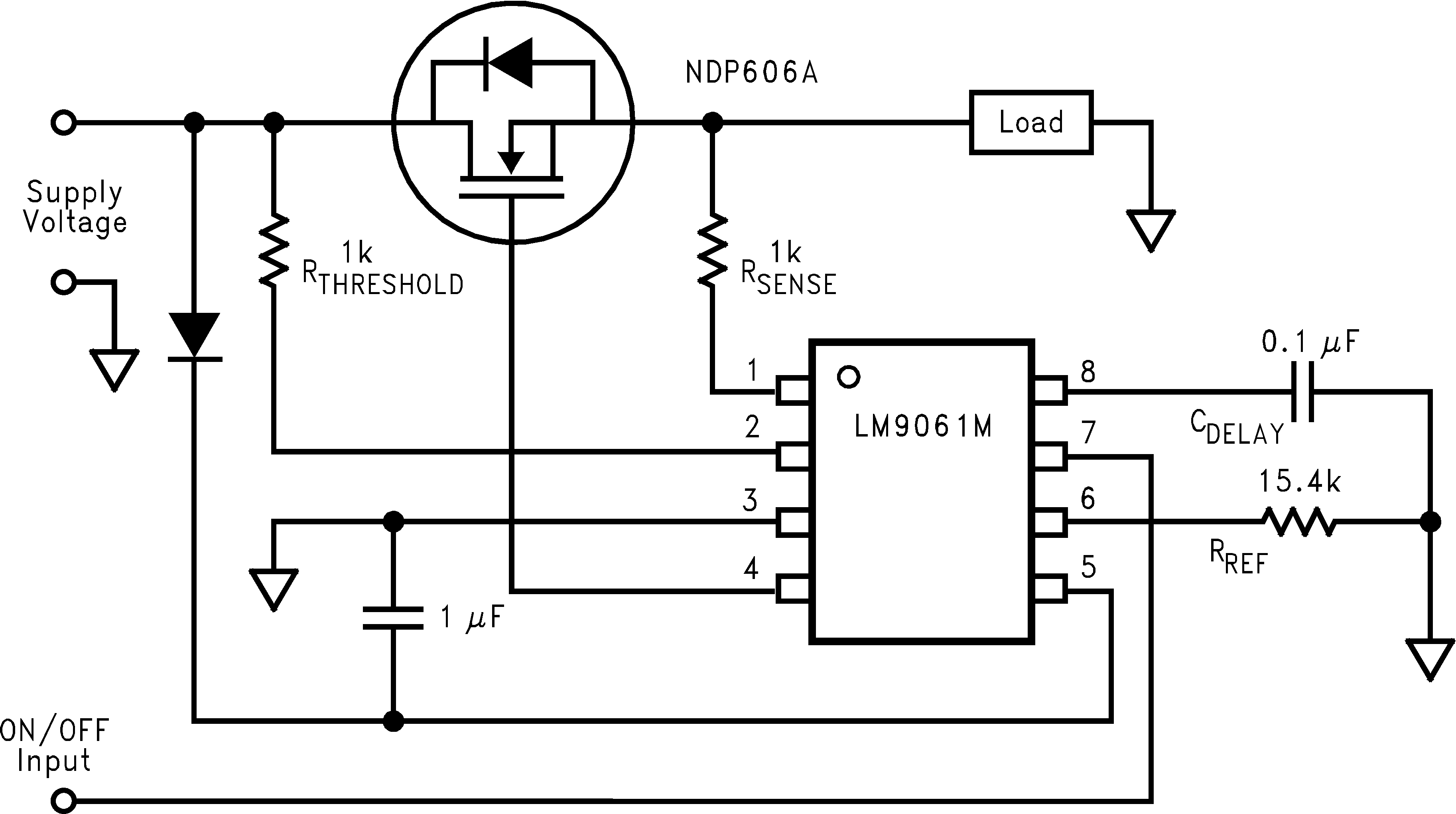
The LM9061 is a charge-pump device which provides the gate drive to an external power MOSFET of any size configured as a high-side driver or switch. This includes multiple parallel connected MOSFETs for very high current applications. A CMOS logic compatible ON/OFF input controls the output gate drive voltage. In the ON state, the charge pump voltage, which is well above the available VCC supply, is directly applied to the gate of the MOSFET. A built-in 15-V Zener clamps the maximum gate to source voltage of the MOSFET. When commanded OFF a 110-µA current sink discharges the gate capacitances of the MOSFET for a gradual turn-OFF characteristic to minimize the duration of inductive load transient voltages and further protect the power MOSFET.
Lossless protection of the power MOSFET is a key feature of the LM9061. The voltage drop (VDS) across the power device is continually monitored and compared against an externally programmable threshold voltage. A small current sensing resistor in series with the load, which causes a loss of available energy, is not required for the protection circuitry. If the VDS voltage, due to excessive load current, exceeds the threshold voltage, the output is latched OFF in a more gradual fashion (through a 10-µA output current sink) after a programmable delay time interval.
| PART NUMBER | PACKAGE | BODY SIZE (NOM) |
|---|---|---|
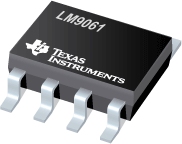
| LM9061/-Q1 | SOIC (8) | 4.9 mm × 3.91 mm |


