


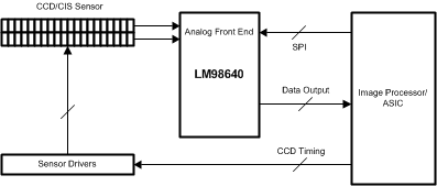


LM98640QML-SP是TI公司的一款CCD/CMOS信号调节产品,LM98640QML-SP是具有 LVDS 输出的双通道、14 位、40 MSPS 模拟前端,本页介绍了LM98640QML-SP的产品说明、应用、特性等,并给出了与LM98640QML-SP相关的TI元器件型号供参考。
LM98640QML-SP - 具有 LVDS 输出的双通道、14 位、40 MSPS 模拟前端 - CCD/CMOS信号调节 - 模拟前端(AFE) - TI公司(Texas Instruments,德州仪器)
- ADC Resolution: 14-Bit
- ADC Sampling Rate: 5 MSPS to 40 MSPS
- Input Level: 2.85 V
- Supply Voltages 3.3Vand 1.8V Nominal
- 125 mW per channel at 15 MSPS
- 178 mW per channet at 40 MSPS
- CDS or S/H Processing for CCD or CIS sensors
- CDS or S/H Gain 0 dB or 6 dB
- Programmable Analog Gain for Each Channel
- 256 Steps; Range -3 dB to 18 dB
- Programmable Analog Offset Correction
- Fine and Coarse DAC Resolution ±8 Bits
- Fine DAC Range ±5 mV
- Coarse DAC Range ±250 mV
- Programmable Input Clamp Voltage
- Programmable Sample Edge: 1/64th Pixel Period
- INL at 15 MHz: ±3.5 LSB
- Noise Floor: -79 dB
- Crosstalk: -80 dB
- Operating Temp: -55°C to +125°C
- Single Event Latch-Up Free to 120 MeV-cm2/mg
- SEFI Free to 120 MeV-cm2/mg
- Total Ionizing Dose: 100 krad(Si)
- Focal Plane Electronics
- Imaging Attitude Control Systems
- Factory Automation Vision Systems
- High-speed Document Scanner
- Multi- Function Peripherals
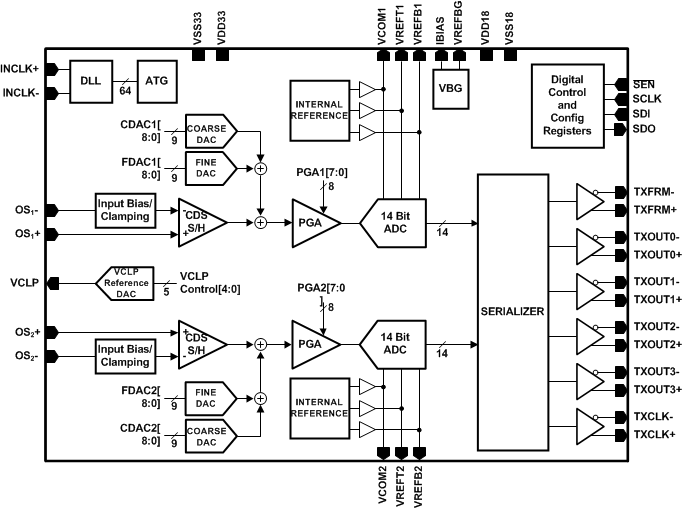
The LM98640QML is a fully integrated, high performance 14-Bit, 5 MSPS to 40 MSPS signal processing solution for image processing applications. The LM98640QML is radiation tolerant up to a total ionizing dose of 100 krad allowing it to be used in space imaging applications. Configuration Registers are Single Event Functional Interrupt Free up to 120 MeV-cm2/mg. The Serial LVDS Output format performs well during single event exposure, preventing data loss. The LM98640QML has an adaptive power scaling feature to optimize power consumption based on the operating frequency and amount of gain required. High-speed signal throughput is achieved with an innovative architecture utilizing Correlated Double Sampling (CDS), typically employed with CCD arrays, or Sample and Hold (S/H) inputs (for CIS and CMOS image sensors). The sampling edges are programmable to a resolution of 1/64th of a pixel period. Both the CDS and S/H have a programmable gain of either 0dB or 6dB. The signal paths utilize two ±8 bit offset correction DACs for coarse and fine offset correction, and 8 bit Programmable Gain Amplifiers (PGA) for each channel. The PGA and offset DAC are programmed independently allowing unique values of gain and offset for each input. The signals are then routed to two on chip 14-bit 40MHz high performance analog-to-digital converters (ADC). The fully differential processing channel provides exceptional noise immunity, having a very low noise floor of -79dB at 1x gain. The 14-bit ADCs have excellent dynamic performance making the LM98640QML transparent in the image reproduction chain.
| PART NUMBER | GRADE | PACKAGE |
|---|---|---|
| LM98640W-MLS | Flight Grade 100 krad | 64 Lead CQFP |
| LM96840W-MPR | Pre-Flight Engineering Protoytpe | 64 Lead CQFP |
| LM98640CVAL | Ceramic Evaluation Board | EVM |
| LM98640-MDR | Flight Grade 100 krad | Die |
| LM98640-MDP | Pre-Flight Engineering Protoytpe | Die |

