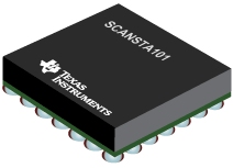

SCANSTA101是TI公司的一款边界扫描(JTAG)接口产品,SCANSTA101是低电压 IEEE 1149.1 系统测试访问 (STA) 主设备,本页介绍了SCANSTA101的产品说明、应用、特性等,并给出了与SCANSTA101相关的TI元器件型号供参考。
SCANSTA101 - 低电压 IEEE 1149.1 系统测试访问 (STA) 主设备 - 边界扫描(JTAG)接口 - 其它接口 - TI公司(Texas Instruments,德州仪器)
The SCANSTA101 is designed to function as a test master for an IEEE 1149.1 boundary scan test system. It is suitable for use in embedded IEEE 1149.1 applications and as a component in a stand-alone boundary scan tester.
The SCANSTA101 is an enhanced version of, and a replacement for, the SCANPSC100. The SCANSTA101 supports the IEEE 1149.1 Test Access Port (TAP) standard and the IEEE 1532 standard for in-system configuration of programmable devices.
The SCANSTA101 improves test vector throughput and reduces software overhead in the system processor. The SCANSTA101 presents a simple, register-based interface to the system processor. Texas Instruments provides C-language source code which can be included in the embedded system software. The combination of the SCANSTA101 and its support software comprises a simple API for boundary scan operations.
The interface from the SCANSTA101 to the system processor is implemented by reading and writing registers, some of which map to locations in the SCANSTA101 memory. Hardware handshaking and interrupt lines are provided as part of the processor interface.
The SCANSTA101 is available as a stand-alone device packaged in a 49-pin NFBGA package. It is also available as an IP macro for synthesis in programmable logic devices.
- Compatible with IEEE Std. 1149.1 (JTAG) Test Access Port and Boundary Scan Architecture
- Supported by Texas Instruments' SCAN Ease (SCAN Embedded Application Software Enabler) Software Rev 2.0
- Uses Generic, Asynchronous Processor Interface; Compatible with a Wide Range of Processors and Processor Clock (PCLK) Frequencies
- 16-Bit Data Interface (IP Scalable to 32-bit)
- 2k x 32 Bit Dual-Port Memory
- Load-on-the-Fly (LotF) and Preloaded Vector Operating Modes Supported
- On-Board Sequencer Allows Multi-Vector Operations such as those Required to Load Data Into an FPGA
- On-Board Compares Support Test Data In (TDI) Validation Against Preloaded Expected Data
- 32-Bit Linear Feedback Shift Register (LFSR) at the Test Data In (TDI) Port for Signature Compression
- State, Shift, and BIST Macros Allow Predetermined Test Mode Select (TMS) Sequences to be Utilized
- Operates at 3.3 V Supply Voltages with 5 V Tolerant I/O
- Outputs Support Power-Down TRI-STATE Mode.


