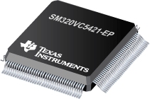

SM320VC5421-EP是TI公司的一款C5000DSP产品,SM320VC5421-EP是增强型产品定点数字信号处理器,本页介绍了SM320VC5421-EP的产品说明、应用、特性等,并给出了与SM320VC5421-EP相关的TI元器件型号供参考。
SM320VC5421-EP - 增强型产品定点数字信号处理器 - C5000DSP - 数字信号处理器 - TI公司(Texas Instruments,德州仪器)
The 320VC5421 fixed-point digital signal processor (DSP) is a dual-core solution running at 200-MIPS performance. The 5421 consists of two DSP subsystems capable of core-to-core communications and a 128K-word zero-wait-state on-chip program memory shared by the two DSP subsystems. Each subsystem consists of one 54x DSP core, 32K-word program/data DARAM, 32K-word data SARAM, 2K-word ROM, three multichannel serial interfaces, xDMA logic, one timer, one APLL, and other miscellaneous circuitry.
The 5421 also contains a host-port interface (HPI) that allows the 5421 to be viewed as a memory-mapped peripheral to a host processor. The 5421 is pin-compatible with the TMS320VC5420.
Each subsystem has its separate program and data spaces, allowing simultaneous accesses to program instructions and data. Two read operations and one write operation can be performed in one cycle. Instructions with parallel store and application-specific instructions can fully utilize this architecture. Furthermore, data can be transferred between program and data spaces. Such parallelism supports a powerful set of arithmetic, logic, and bit-manipulation operations that can all be performed in a single machine cycle. The 5421 includes the control mechanisms to manage interrupts, repeated operations, and function calls. In addition, the 5421 has 128K words of on-chip program memory that can be shared between the two subsystems.
The 5421 is intended as a high-performance, low-cost, high-density DSP for remote data access or voice-over IP subsystems. It is designed to maintain the current modem architecture with minimal hardware and software impacts, thus maximizing reuse of existing modem technologies and development efforts.
- Controlled Baseline
- One Assembly/Test Site, One Fabrication Site
- Extended Temperature Performance of –40°C to 85°C
- Enhanced Diminishing Manufacturing Sources (DMS) Support
- Enhanced Product-Change Notification
- Qualification Pedigree
- 200-MIPS Dual-Core DSP Consisting of Two Independent Subsystems
- Each Core Has an Advanced Multibus Architecture With Three Separate 16-Bit Data Memory Buses and One Program Bus
- 40-Bit Arithmetic Logic Unit (ALU) Including a 40-Bit Barrel-Shifter and Two 40-Bit Accumulators Per Core
- Each Core Has a 17-Bit × 17-Bit Parallel Multiplier Coupled to a 40-Bit Adder for Non-Pipelined Single-Cycle Multiply/Accumulate (MAC) Operations
- Each Core Has a Compare, Select, and Store Unit (CSSU) for the Add/Compare Selection of the Viterbi Operator
- Each Core Has an Exponent Encoder to Compute an Exponent Value of a 40-Bit Accumulator Value in a Single Cycle
- Each Core Has Two Address Generators With Eight Auxiliary Registers and Two Auxiliary Register Arithmetic Units (ARAUs)
- 16-Bit Data Bus With Data Bus Holder Feature
- 512K-Word × 16-Bit Extended Program Address Space
- Total of 256K-Word × 16-Bit Dual- and Single-Access On-Chip RAM (128K-Word x 16-Bit Two-Way Shared Memory)
- Single-Instruction Repeat and Block-Repeat Operations
- Instructions With 32-Bit-Long Word Operands
- Instructions With Two or Three Operand Reads
- Fast Return From Interrupts
- Arithmetic Instructions With Parallel Store and Parallel Load
- Conditional Store Instructions
- Output Control of CLKOUT
- Output Control of TOUT
- Power Consumption Control With IDLE1, IDLE2, and IDLE3 Instructions
- Dual 1.8-V (Core) and 3.3-V (I/O) Power Supplies for Low-Power, Fast Operations
- 10-ns Single-Cycle Fixed-Point Instruction
- Interprocessor Communication via Two Internal 8-Element FIFOs
- Twelve Channels of Direct Memory Access (DMA) for Data Transfers With No CPU Loading (Six Channels Per Subsystem With External Access)
- Six Multichannel Buffered Serial Ports (McBSPs) With 128-Channel Selection Capability (Three McBSPs per Subsystem)
- 16-Bit Host-Port Interface (HPI) Multiplexed With External Memory Interface Pins
- Software-Programmable Phase-Locked Loop (APLL) Provides Several Clocking Options (Requires External Oscillator)
- On-Chip Scan-Based Emulation Logic, IEEE Standard 1149-1 (JTAG) Boundary-Scan Logic
- Two Software-Programmable Timers (One Per Subsystem)
- Software-Programmable Wait-State Generator (14 Wait States Maximum)
- Provided in 144-pin Low-Profile Quad Flatpack (LQFP) (PGE Suffix) Package
Component qualification in accordance with JEDEC and industry standards to ensure reliable operation over an extended temperature range. This includes, but is not limited to, Highly Accelerated Stress Test (HAST) or biased 85/85, temperature cycle, autoclave or unbiased HAST, electromigration, bond intermetallic life, and mold compound life. Such qualification testing should not be viewed as justifying use of this component beyond specified performance and environmental limits. IEEE Standard 1149.1-1990 Standard-Test-Access Port and Boundary Scan Architecture.


