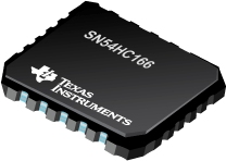

SN54HC166是TI公司的一款移位寄存器产品,SN54HC166是并联负载 8 位移位寄存器,本页介绍了SN54HC166的产品说明、应用、特性等,并给出了与SN54HC166相关的TI元器件型号供参考。
SN54HC166 - 并联负载 8 位移位寄存器 - 移位寄存器 - 触发器/锁存器/寄存器 - TI公司(Texas Instruments,德州仪器)
These parallel-in or serial-in, serial-out registers feature gated clock (CLK, CLK INH) inputs and an overriding clear (CLR)\ input. The parallel-in or serial-in modes are established by the shift/load (SH/LD)\ input. When high, SH/LD\ enables the serial (SER) data input and couples the eight flip-flops for serial shifting with each clock (CLK) pulse. When low, the parallel (broadside) data inputs are enabled, and synchronous loading occurs on the next clock pulse. During parallel loading, serial data flow is inhibited. Clocking is accomplished on the low-to-high-level edge of CLK through a 2-input positive-NOR gate permitting one input to be used as a clock-enable or clock-inhibit function. Holding either CLK or CLK INH high inhibits clocking; holding either low enables the other clock input. This allows the system clock to be free running, and the register can be stopped on command with the other clock input. CLK INH should be changed to the high level only when CLK is high. CLR\ overrides all other inputs, including CLK, and resets all flip-flops to zero.
- Wide Operating Voltage Range of 2 V to 6 V
- Outputs Can Drive Up To 10 LSTTL Loads
- Low Power Consumption, 80-µA Max ICC
- Typical tpd = 13 ns
- ±4-mA Output Drive at 5 V
- Low Input Current of 1 µA Max
- Synchronous Load
- Direct Overriding Clear
- Parallel-to-Serial Conversion


