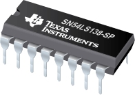

SN54LS138-SP是TI公司的一款解码器/编码器/多路复用器产品,SN54LS138-SP是3 线路至 8 线路解码器/多路解复用器,本页介绍了SN54LS138-SP的产品说明、应用、特性等,并给出了与SN54LS138-SP相关的TI元器件型号供参考。
SN54LS138-SP - 3 线路至 8 线路解码器/多路解复用器 - 解码器/编码器/多路复用器 - 特殊逻辑 - TI公司(Texas Instruments,德州仪器)
These Schottky-clamped TTL MSI circuits are designed to be used in high-performance memory decoding or data-routing applications requiring very short propagation delay times. In high-performance memory systems, these decoders can be used to minimize the effects of system decoding. When employed with high-speed memories utilizing a fast enable circuit, the delay times of these decoders and the enable time of the memory are usually less than the typical access time of the memory. This means that the effective system delay introduced by the Schottky-clamped system decoder is negligible.
The 'LS138, SN54S138, and SN74S138A decode one of eight lines dependent on the conditions at the three binary select inputs and the three enable inputs. Two active-low and one active-high enable inputs reduce the need for external gates or inverters when expanding. A 24-line decoder can be implemented without external inverters and a 32-line decoder requires only one inverter. An enable input can be used as a data input for demultiplexing applications.
All of these decoder/demultiplexers feature fully buffered inputs, each of which represents only one normalized load to its driving circuit. All inputs are clamped with high-performance Schottky diodes to suppress line-ringing and to simplify system design.
The SN54LS138 and SN54S138 are characterized for operation over the full military temperature range of -55°C to 125°C. The SN74LS138 and SN74S138A are characterized for operation from 0°C to 70°C.
- Designed Specifically for High-Speed:
- Memory Decoders
- Data Transmission Systems
- 3 Enable Inputs to Simplify Cascading and/or Data Reception
- Schottky-Clamped for High Performance


