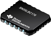

SN55LBC176是TI公司的一款无产品,SN55LBC176是差动总线收发器,本页介绍了SN55LBC176的产品说明、应用、特性等,并给出了与SN55LBC176相关的TI元器件型号供参考。
SN55LBC176 - 差动总线收发器 - 无 - RS-485收发器 - TI公司(Texas Instruments,德州仪器)
The SN55LBC176, SN65LBC176, SN65LBC176Q, and SN75LBC176 differential bus transceivers are monolithic, integrated circuits designed for bidirectional data communication on multipoint bus-transmission lines. They are designed for balanced transmission lines and meet ANSI Standard TIA/EIA-485-A (RS-485) and ISO 8482:1987(E).
The SN55LBC176, SN65LBC176, SN65LBC176Q, and SN75LBC176 combine a 3-state, differential line driver and a differential input line receiver, both of which operate from a single 5-V power supply. The driver and receiver have active-high and active-low enables, respectively, which can externally connect together to function as a direction control. The driver differential outputs and the receiver differential inputs connect internally to form a differential input/output (I/O) bus port that is designed to offer minimum loading to the bus whenever the driver is disabled or VCC = 0. This port features wide positive and negative common-mode voltage ranges, making the device suitable for party-line applications. Very low device supply current can be achieved by disabling the driver and the receiver.
These transceivers are suitable for ANSI Standard TIA/EIA-485 (RS-485) and ISO 8482 applications to the extent that they are specified in the operating conditions and characteristics section of this data sheet. Certain limits contained in TIA/EIA-485-A and ISO 8482:1987 (E) are not met or cannot be tested over the entire military temperature range.
The SN55LBC176 is characterized for operation from –55°C to 125°C. The SN65LBC176 is characterized for operation from –40°C to 85°C, and the SN65LBC176Q is characterized for operation from –40°C to 125°C. The SN75LBC176 is characterized for operation from 0°C to 70°C.
- Bidirectional Transceiver
- Meets or Exceeds the Requirements of ANSI Standard TIA/EIA.485.A and ISO 8482:1987(E)
- High-Speed Low-Power LinBiCMOS™ Circuitry
- Designed for High-Speed Operation in Both Serial and Parallel Applications
- Low Skew
- Designed for Multipoint Transmission on Long Bus Lines in Noisy Environments
- Very Low Disabled Supply Current . . . 200 µA Maximum
- Wide Positive and Negative Input/Output Bus Voltage Ranges
- Thermal-Shutdown Protection
- Driver Positive-and Negative-Current Limiting
- Open-Circuit Failsafe Receiver Design
- Receiver Input Sensitivity . . . ±200 mV Max
- Receiver Input Hysteresis . . . 50 mV Typ
- Operates From a Single 5-V Supply
- Glitch-Free Power-Up and Power-Down Protection
- Available in Q-Temp Automotive HighRel Automotive ApplicationsConfiguration Control / Print Support Qualification to Automotive Standards
LinBiCMOS and LinASIC are trademarks of Texas Instruments Incorporated.


