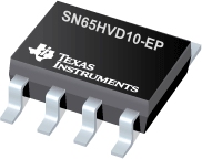

SN65HVD10-EP是TI公司的一款无产品,SN65HVD10-EP是增强型产品 3.3V RS-485 收发器,本页介绍了SN65HVD10-EP的产品说明、应用、特性等,并给出了与SN65HVD10-EP相关的TI元器件型号供参考。
SN65HVD10-EP - 增强型产品 3.3V RS-485 收发器 - 无 - RS-485收发器 - TI公司(Texas Instruments,德州仪器)
- Controlled Baseline
- One Assembly/Test Site
- One Fabrication Site
- Extended Temperature Performance of Up to -40°C to 125°C and -55°C to 125°C
- Enhanced Diminishing Manufacturing Sources (DMS) Support
- Enhanced Product-Change Notification
- Qualification Pedigree(1)
- Operates With a 3.3 V Supply
- Bus-Pin ESD Protection Exceeds 16 kV HBM
- 1/8 Unit-Load Option Available (Up to 256 Nodes on the Bus)
- Optional Driver Output Transition Times for Signaling Rates of 1 Mbps, 10 Mbps, and 25 Mbps(2)
- Meets or Exceeds the Requirements of ANSI TIA/EIA-485-A
- Bus-Pin Short Circuit Protection From -7 V to 12 V
- Low-Current Standby Mode . . . 1 µA (Typ)
- Open-Circuit, Idle-Bus, and Shorted-Bus Failsafe Receiver
- Thermal Shutdown Protection
- Glitch-Free Power-Up and Power-Down Protection for Hot-Plugging Applications
- SN75176 Footprint
- APPLICATIONS
- Digital Motor Control
- Utility Meters
- Chassis-to-Chassis Interconnects
- Electronic Security Stations
- Industrial Process Control
- Building Automation
- Point-of-Sale (POS) Terminals and Networks
(1) Component qualification in accordance with JEDEC and industry standards to ensure reliable operation over an extended temperature range. This includes, but is not limited to, Highly Accelerated Stress Test (HAST) or biased 85/85, temperature cycle, autoclave or unbiased HAST, electromigration, bond intermetallic life, and mold compound life. Such qualification testing should not be viewed as justifying use of this component beyond specified performance and environmental limits.(2) The signaling rate of a line is the number of voltage transitions that are made per second expressed in the units bps (bits per second).
DESCRIPTION/ORDERING INFORMATION
The SN65HVD10, SN65HVD11, and SN65HVD12 combine a 3-state differential line driver and differential input line receiver that operate with a single 3.3 V power supply. They are designed for balanced transmission lines and meet or exceed ANSI standard TIA/EIA-485-A and ISO 8482:1993. These differential bus transceivers are monolithic integrated circuits designed for bidirectional data communication on multipoint bus-transmission lines. The drivers and receivers have active-high and active-low enables respectively, that can be externally connected together to function as direction control. Low device standby supply current can be achieved by disabling the driver and the receiver.
The driver differential outputs and receiver differential inputs connect internally to form a differential input/output (I/O) bus port that is designed to offer minimum loading to the bus whenever the driver is disabled or VCC = 0. These parts feature wide positive and negative common-mode voltage ranges, making them suitable for party-line applications.


