
SN65HVD1787是TI公司的一款无产品,SN65HVD1787是具有故障保护功能的 30V RS-485,共模范围从 -20 至 +25,本页介绍了SN65HVD1787的产品说明、应用、特性等,并给出了与SN65HVD1787相关的TI元器件型号供参考。
SN65HVD1787 - 具有故障保护功能的 30V RS-485,共模范围从 -20 至 +25 - 无 - RS-485收发器 - TI公司(Texas Instruments,德州仪器)
- Bus-Pin Fault Protection to:
- > ±70 V ('HVD1785, 86, 91, 92)
- > ±30 V ('HVD1787, 93)
- Common-Mode Voltage Range (–20 V to 25 V) More Than Doubles TIA/EIA 485 Requirement
- Bus I/O Protection
- ±16 kV JEDEC HBM Protection
- Reduced Unit Load for Up to 256 Nodes
- Failsafe Receiver for Open-Circuit, Short-Circuit and Idle-Bus Conditions
- Low Power Consumption
- Low Standby Supply Current, 1 μA Typical
- ICC 5 mA Quiescent During Operation
- Power-Up, Power-Down Glitch-Free Operation
- Designed for RS-485 and RS-422 Networks
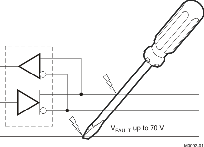
These devices are designed to survive overvoltage faults such as direct shorts to power supplies, mis-wiring faults, connector failures, cable crushes, and tool mis-applications. They are also robust to ESD events, with high levels of protection to human-body model specifications.
These devices combine a differential driver and a differential receiver, which operate from a single power supply. In the 'HVD1785, 'HVD1786, and 'HVD1787, the driver differential outputs and the receiver differential inputs are connected internally to form a bus port suitable for half-duplex (two-wire bus) communication. In the 'HVD1793, the driver differential outputs and the receiver differential inputs are separate pins, to form a bus port suitable for full-duplex (four-wire bus) communication. These ports feature a wide common-mode voltage range, making the devices suitable for multipoint applications over long cable runs. These devices are characterized from –40°C to 105°C.
For similar features with 3.3-V supply operation, see the SN65HVD1781 (SLLS877).
| PART NUMBER | PACKAGE | BODY SIZE (NOM) |
|---|---|---|
| SN65HVD1785, SN65HVD1786, SN65HVD1787 | SOIC (8) | 4.90 mm × 3.91 mm |
| PDIP (8) | 9.81 mm × 6.35 mm | |
| SN65HVD1791, SN65HVD1792, SN65HVD1793 | SOIC (14) | 8.65 mm × 3.91 mm |


