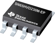

SN65HVD230M-EP是TI公司的一款无产品,SN65HVD230M-EP是具有待机模式的增强型产品 3.3V Can 收发器,本页介绍了SN65HVD230M-EP的产品说明、应用、特性等,并给出了与SN65HVD230M-EP相关的TI元器件型号供参考。
SN65HVD230M-EP - 具有待机模式的增强型产品 3.3V Can 收发器 - 无 - CAN收发器 - TI公司(Texas Instruments,德州仪器)
The SN65HVD230M controller area network (CAN) transceiver is designed for use with the Texas Instruments TMS320Lx240x 3.3-V DSPs with CAN controllers, or with equivalent devices. They are intended for use in applications employing the CAN serial communication physical layer in accordance with the ISO 11898 standard. Each CAN transceiver is designed to provide differential transmit capability to the bus and differential receive capability to a CAN controller at speeds up to 1 Mbps.
Designed for operation in especially-harsh environments, these devices feature cross-wire protection, loss-of-ground and overvoltage protection, overtemperature protection, as well as wide common-mode range.
The transceiver interfaces the single-ended CAN controller with the differential CAN bus found in industrial, building automation, and automotive applications. It operates over a -2-V to 7-V common-mode range on the bus and it can withstand common-mode transients of ±25 V.
On the SN65HVD230M, RS (pin 8) provides three different modes of operation: high-speed, slope control, and low-power modes. The high-speed mode of operation is selected by connecting pin 8 to ground, allowing the transmitter output transistors to switch on and off as fast as possible with no limitation on the rise and fall slopes. The rise and fall slopes can be adjusted by connecting a resistor to ground at pin 8, since the slope is proportional to the pin’s output current. This slope control is implemented with external resistor values of 10 k, to achieve a 2-V/µs slew rate.
The circuit of the SN65HVD230M enters a low-current standby mode during which the driver is switched off and the receiver remains active if a high logic level is applied to RS (pin 8). The DSP controller reverses this low-current standby mode when a dominant state (bus differential voltage > 900 mV typical) occurs on the bus.
The Vref (pin 5 on the SN65HVD230M) is available as a VCC/2 voltage reference.
- Controlled Baseline
- One Assembly/Test Site, One Fabrication Site
- Extended Temperature Performance of -55°C to 125°C
- Enhanced Diminishing Manufacturing Sources (DMS) Support
- Enhanced Product-Change Notification
- Qualification Pedigree
- Operates With a 3.3-V Supply
- Low Power Replacement for the PCA82C250 Footprint
- Bus/Pin ESD Protection Exceeds 15-kV HBM
- Controlled Driver Output Transition Times for Improved Signal Quality on the SN65HVD230M
- Unpowered Node Does Not Disturb the Bus
- Compatible With the Requirements of the ISO 11898 Standard
- Low-Current SN65HVD230M Standby Mode 370 µA Typical
- Designed for Signaling Rates Up To 1 Megabit/Second (Mbps)
- Thermal Shutdown Protection
- Open-Circuit Fail-Safe Design
Component qualification in accordance with JEDEC and industry standards to ensure reliable operation over an extended temperature range. This includes, but is not limited to, Highly Accelerated Stress Test (HAST) or biased 85/85, temperature cycle, autoclave or unbiased HAST, electromigration, bond intermetallic life, and mold compound life. Such qualification testing should not be viewed as justifying use of this component beyond specified performance and environmental limits. The signaling rate of a line is the number of voltage transitions that are made per second expressed in the units bps (bits per second).


